Micro-nano structure and morphology measurement device and method based on digital scanning and white light interference

A technology of micro-nano structure and topography measurement, applied in measurement devices, optical devices, instruments, etc., to achieve the effect of improving anti-interference ability, reducing influence and simplifying system structure

Active Publication Date: 2014-07-02
INST OF OPTICS & ELECTRONICS - CHINESE ACAD OF SCI
View PDF5 Cites 26 Cited by
  • Summary
  • Abstract
  • Description
  • Claims
  • Application Information

AI Technical Summary

Problems solved by technology

[0004] The purpose of the present invention is to solve the problems existing in the existing white light interferometry technology, and to provide a micro-nano structure shape measurement device based on the principle of white light interferometry that does not need to scan in the z direction and has high anti-interference ability and high measurement accuracy. method

Method used


Image

  • Micro-nano structure and morphology measurement device and method based on digital scanning and white light interference
  • Micro-nano structure and morphology measurement device and method based on digital scanning and white light interference
  • Micro-nano structure and morphology measurement device and method based on digital scanning and white light interference

Examples


Embodiment Construction

[0019] In order to make the object, technical solution and advantages of the present invention clearer, the present invention will be described in further detail below in conjunction with specific embodiments and with reference to the accompanying drawings.

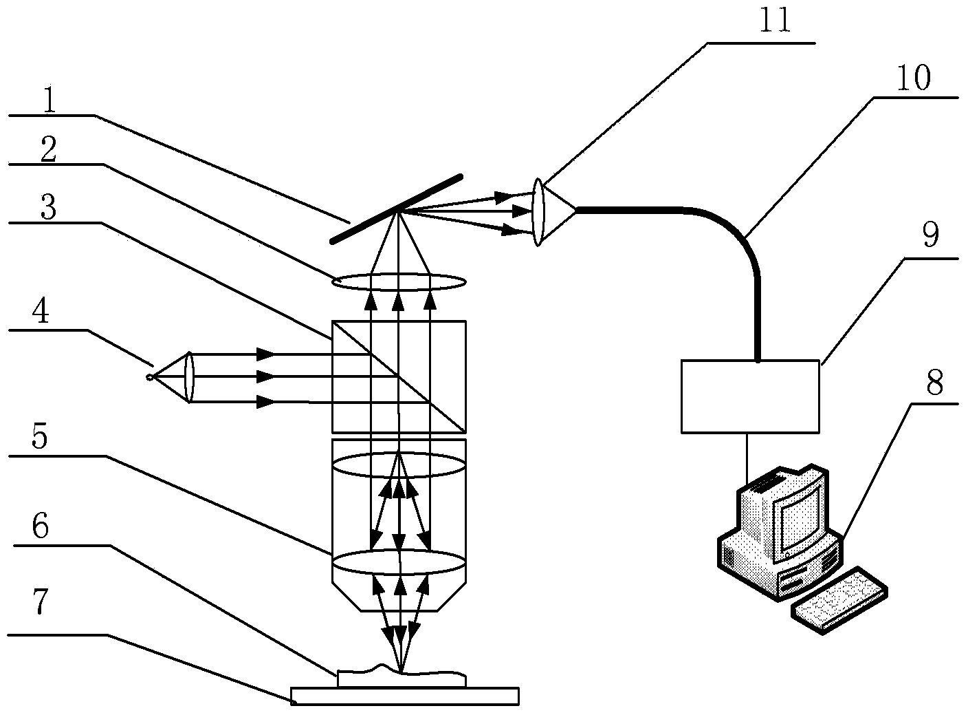
[0020] as attached figure 1 Shown is a schematic diagram of the structure of the micro-nano structure profile measurement device based on digital scanning white light interference of the present invention, a digital micromirror array (DMD) 1, an imaging unit 2, a half mirror 3, a white light source 4, and an interference microscope objective lens 5 , an object to be measured 6, a workpiece table 7, a control unit 8, a spectrometer 9, an optical fiber 10, an optical fiber coupling unit 11; a digital micromirror array 1, an imaging unit 2, a half mirror 3, an interference microscope objective lens 5 and the The object 6 is sequentially located on the optical axis of the micro-nano structure topography measuring device; the ...


PUM


Abstract

The invention provides a micro-nano structure and morphology measurement device and method based on digital scanning and white light interference. The method includes the steps of projecting white light processed through beam expanding and collimation to the surface of an object to the measured and the surface of a reference mirror inside an interference microscope through semi-transparent and semi-reflective mirrors by means of a device composed of a digital micro mirror array, an imaging unit, the semi-transparent and semi-reflective mirrors, a white light source, an interference microscope objective, the object to be measured, a working table, a control unit, a spectrograph, optical fibers and an optical fiber coupling unit, enabling the white light to interfere with reflected light, obtaining the interference light intensities through the semi-transparent and semi-reflective mirrors, obtaining the surface of the digital micro mirror array through the imaging unit, controlling the micro mirror defection angles corresponding to pixels of the digital micro mirror array one by one so that the light intensities corresponding to different pixels can enter the optical fiber coupling unit one by one, transmitting spectral information obtained by a spectrograph and corresponding to the interference light intensities to the control unit, and conducting phase analysis on distribution of the spectrums corresponding to the interference light intensities to obtain the relative height of the surface of the object to be measured. The micro-nano structure and morphology measurement device and method have the advantages that the structure is simplified, the measurement accuracy is high, and the anti-interference capacity is high.

Description

technical field [0001] The invention belongs to the technical field of optical precision detection, and relates to an optical non-contact measurement method, in particular to a measurement device and method for micro-nano structure surface appearance based on white light frequency domain analysis. Background technique [0002] With the wide application of micro-nano devices such as MEMS, in order to ensure the performance of the device, high requirements are put forward for the micro-nano structure shape measurement technology. Among the existing microstructure shape measurement technologies, white light interferometry has become the mainstream technology due to its advantages of large measurement range and high precision. However, most of the existing technologies for measuring the morphology of micro-nano structures based on the principle of white light interference scan the object to be measured in the z-direction by moving the workpiece stage or interference microscope i...

Claims


Application Information

Patent Timeline
Patent Type & Authority Applications(China)
IPC IPC(8): G01B11/24
Inventor 唐燕何渝赵立新朱江平胡松
Owner INST OF OPTICS & ELECTRONICS - CHINESE ACAD OF SCI
Why Eureka
Try Eureka