Silicon-based CMOS image sensor and method for improving electron transfer efficiency of silicon-based CMOS image sensor

A technology of image sensor and transfer efficiency, which is applied in the field of microelectronics to achieve the effect of improving transfer efficiency, solving noise problems and improving characteristics

Inactive Publication Date: 2014-07-02
FUDAN UNIV
View PDF8 Cites 17 Cited by
  • Summary
  • Abstract
  • Description
  • Claims
  • Application Information

AI Technical Summary

Problems solved by technology

However, since the N-type doping concentration of point A is higher than that of point B, the potential of point A is higher than that of point B, so there is a potential barrier between A and B

Method used


Image

  • Silicon-based CMOS image sensor and method for improving electron transfer efficiency of silicon-based CMOS image sensor
  • Silicon-based CMOS image sensor and method for improving electron transfer efficiency of silicon-based CMOS image sensor
  • Silicon-based CMOS image sensor and method for improving electron transfer efficiency of silicon-based CMOS image sensor

Examples


Embodiment Construction

[0034] Below in conjunction with accompanying drawing and embodiment, further describe the present invention.

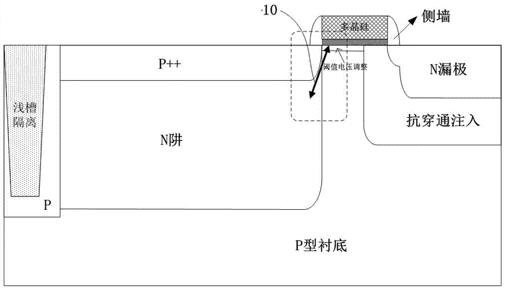
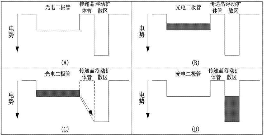
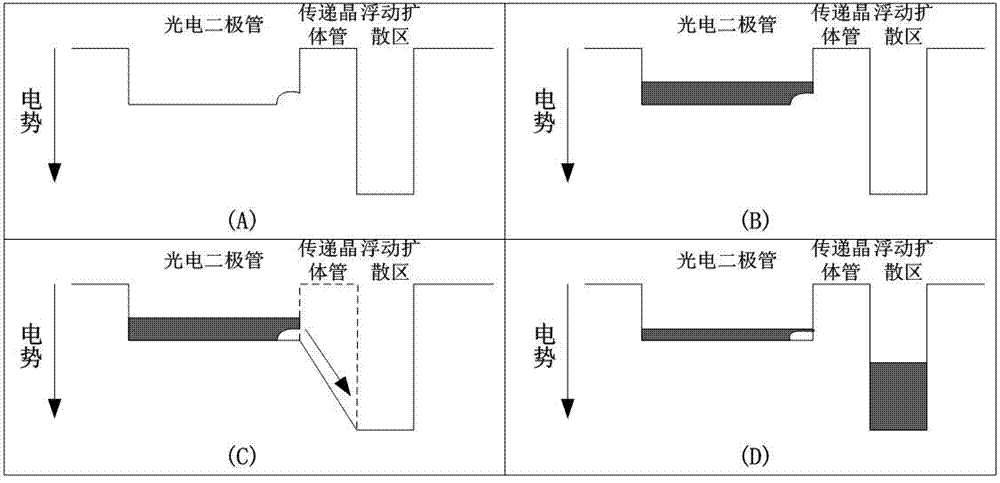
[0035] The present invention is different from the traditional silicon-based CMOS image sensor in that the photosensitive region (PPD) and the channel connection part of the transfer transistor (TX) are distributed in increasing doping concentration from the body to the surface, which can be formed by the following two methods:

[0036] 1. After the other parts of the silicon-based CMOS image sensor are formed, a photolithography plate is used to implant P-type ions with different energies and concentrations in the channel connection area between the photosensitive area (PPD) and the transfer transistor (TX) for multiple times;

[0037] 2. N-type ions with different energies and different concentrations are continuously injected multiple times to obtain the photo-generated electron collection area in the photosensitive area, forming a gradual decrease in N-type doping...


PUM


Abstract

The invention belongs to the technical field of microelectronics, and particularly relates to a silicon-based CMOS image sensor and a method for improving electron transfer efficiency of the silicon-based CMOS image sensor. According to the silicon-based CMOS image sensor and the method for improving the electron transfer efficiency of the silicon-based CMOS image sensor, due to the fact that increasing doping from the interior to the surface is led into the portion where a light sensing area makes contact with a transfer transistor (TX) channel area, the electric potential is gradually increased from the interior of a substrate to the TX surface channel, photon-generated carriers can be completely transferred, the theoretical limit of the number of the transferred carriers can be met, and the problem of noise caused by incomplete transfer of the photon-generated carriers is successfully solved.

Description

technical field [0001] The invention belongs to the technical field of microelectronics, and in particular relates to a silicon-based CMOS image sensor and a method for improving electron transfer efficiency. Background technique [0002] Image sensors are semiconductor devices that convert optical images into electrical signals, and can generally be divided into CMOS image sensors and CCD image sensors. CMOS image sensor has been the research hotspot of image sensor in the past ten years. Compared with traditional CCD image sensor, CMOS image sensor has the advantages of small size, low power consumption and low cost, and because of its compatibility with CMOS process, CMOS image sensor A powerful system-on-chip can be realized. [0003] The single pixel structure of a traditional CMOS image sensor such as figure 1 shown. It is mainly composed of a photodiode (PPD), a floating diffusion (FD) and a transfer transistor (TX). [0004] Ideally, the working principle of a si...

Claims


Application Information

Patent Timeline
Patent Type & Authority Applications(China)
IPC IPC(8): H01L27/146
Inventor 蒋玉龙包永霞
Owner FUDAN UNIV
Why Eureka
Try Eureka