Middle-infrared band broadband cycle wave-absorbing material

A wave-absorbing material and infrared band technology, applied in optical components, optics, instruments, etc., can solve the problems of single frequency band and narrow absorption frequency band, and achieve the effect of expanding bandwidth, wide absorption frequency band, and easy realization

Active Publication Date: 2014-07-09
UNIV OF ELECTRONICS SCI & TECH OF CHINA
View PDF4 Cites 12 Cited by
  • Summary
  • Abstract
  • Description
  • Claims
  • Application Information

AI Technical Summary

Problems solved by technology

However, since this absorption effect is based on the electromagnetic resonance characteristics of the periodic perfect absorbing structure, the single frequency band and narrow absorption frequency band are its inherent defects.

Method used


Image

  • Middle-infrared band broadband cycle wave-absorbing material
  • Middle-infrared band broadband cycle wave-absorbing material
  • Middle-infrared band broadband cycle wave-absorbing material

Examples


specific Embodiment approach 1

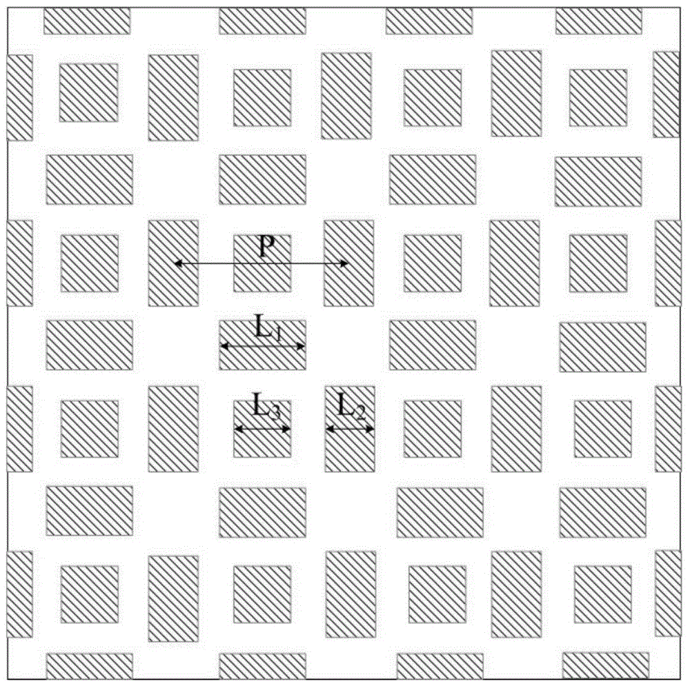
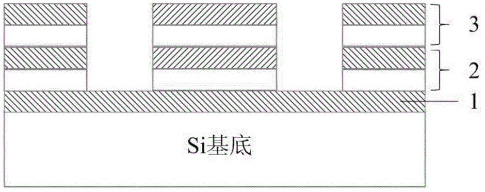
[0027] like figure 2 As shown, a double-layer "metal-dielectric" resonant layer structure and a periodic absorbing structure composed of a continuous metal film on the bottom layer are used to realize the broadband absorbing structure BM-1. On the supporting Si substrate, there is first a continuous metal Al thin film 1 with a thickness of 100nm, and a double-layer "metal-medium" resonant layer structure on it. The medium in the lower resonance layer 2 is Y with a thickness of 100nm 2 o 3 thin film, the real part of its dielectric constant is 3.21, and the medium in the upper resonant layer 3 is Al with a thickness of 150nm 2 o 3 The real part of the dielectric constant of the thin film is 2.28, and the thickness of the metal patch layer in the two resonant layers is both 50nm. The period of BM-1 is P=4.7μm, and the size of the patch in the resonant unit is L 1 =1.7μm, L 2 =1.5μm, L 3 =1.6μm. Its absorption rate curve is as Figure 4 As shown in the figure, it can be...

specific Embodiment approach 2

[0028] like figure 2 As shown, a double-layer "metal-dielectric" resonant layer structure and a periodic absorbing structure composed of a continuous metal film on the bottom layer are used to realize the broadband absorbing structure BM-2. On the supporting Si substrate, there is first a continuous metal Al film with a thickness of 100nm, and a double-layer "metal-medium" resonant layer structure on it. The medium in the lower resonance layer is Al with a thickness of 100nm 2 o 3 Thin film, the real part of its dielectric constant is 2.28, and the medium in the upper resonant layer is MgF with a thickness of 150nm 2 The real part of the dielectric constant of the thin film is 1.75, and the thickness of the metal patch layer in the two resonant layers is both 50nm. The period of BM-1 is P=4.7μm, and the size of the patch in the resonant unit is L 1 =1.7μm, L 2 =1.5μm, L 3 =1.6μm. Its absorption rate curve is as Figure 5 As shown, it can be seen from the figure that d...

specific Embodiment approach 3

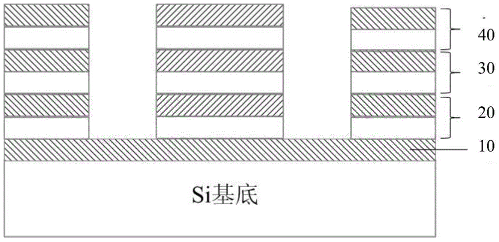
[0029] like image 3 As shown, a three-layer "metal-dielectric" resonant layer structure and a periodic absorbing structure composed of a continuous metal film on the bottom layer are used to realize the broadband absorbing structure BM-3. On the supporting Si substrate substrate, there is first a continuous metal Al film 1 with a thickness of 100nm 0 , above which is a three-layer "metal-dielectric" resonant layer structure. Bottom resonant layer 2 0 The medium in the medium is MgF with a thickness of 150nm 2 Thin film, the real part of its dielectric constant is 1.75, the middle resonant layer 3 0 The medium in the medium is Al with a thickness of 100nm 2 o 3 thin film with a real part of the dielectric constant of 2.28 and a top resonant layer of 4 0 The medium in the medium is Y with a thickness of 150nm 2 o 3 The real part of the dielectric constant of the thin film is 3.21, and the thickness of the metal patch layer in the three resonant layers is 50nm. The peri...


PUM


Abstract

The invention discloses a middle-infrared band broadband cycle wave-absorbing material, and belongs to the technical field of function materials and devices. The middle-infrared band broadband cycle wave-absorbing material comprises an underlying metal film and a graphical resonance wave-absorbing layer arranged on the underlying metal film. The middle-infrared band broadband cycle wave-absorbing material is characterized in that the resonance wave-absorbing layer at least comprises two overlapped resonance layers, each resonance layer comprises a dielectric layer and a metal layer, and the dielectric constant values of the dielectric layer materials of the resonance layers are sequentially increased or decreased. According to the middle-infrared band broadband cycle wave-absorbing material, due to the fact that broadband absorption peaks of the resonance layers are overlapped, the bandwidth of the absorption peaks is extremely expanded, and more incident wave energy can be obtained from given wavebands.

Description

technical field [0001] The invention belongs to the technical field of functional materials and devices, and relates to an infrared periodic wave-absorbing structure, which is applied to multiple fields such as infrared camouflage, infrared lattice imaging, infrared radiation energy control, and infrared photoelectric devices. Background technique [0002] Periodic perfect absorber is a new type of electromagnetic structural device derived from electromagnetic metamaterial in recent years. This periodic absorbing structure utilizes the resonance characteristics of metamaterials: the incident electric field and the metal array unit generate electrical resonance, and an antiparallel current is induced between the upper and lower parallel layers of metal, resulting in a magnetic resonance between the incident magnetic field and the induced magnetic field, thereby So that the electromagnetic wave is effectively localized in the unit structure. According to the equivalent coal q...

Claims


Application Information

Patent Timeline
Patent Type & Authority Applications(China)
IPC IPC(8): G02B5/00
Inventor 邓龙江张楠周佩珩陈良谢建良
Owner UNIV OF ELECTRONICS SCI & TECH OF CHINA
Why Eureka
Try Eureka