Semiconductor lead frame manufacturing technology

A technology of lead frame and manufacturing process, which is applied in the field of semiconductor lead frame manufacturing technology, can solve the problems of poor quality of lead frame and large amount of precious metals, etc., and achieve the effects of strong coating adhesion, reasonable arrangement of process steps, and strong protection

Active Publication Date: 2014-07-16
SICHUAN JINWAN ELECTRONICS
View PDF8 Cites 17 Cited by
  • Summary
  • Abstract
  • Description
  • Claims
  • Application Information

AI Technical Summary

Problems solved by technology

[0005] In order to overcome the defects of the large amount of precious metal used and the poor quality of the manufactured lead frame, th...

Method used


Image

  • Semiconductor lead frame manufacturing technology
  • Semiconductor lead frame manufacturing technology
  • Semiconductor lead frame manufacturing technology

Examples


Embodiment 1

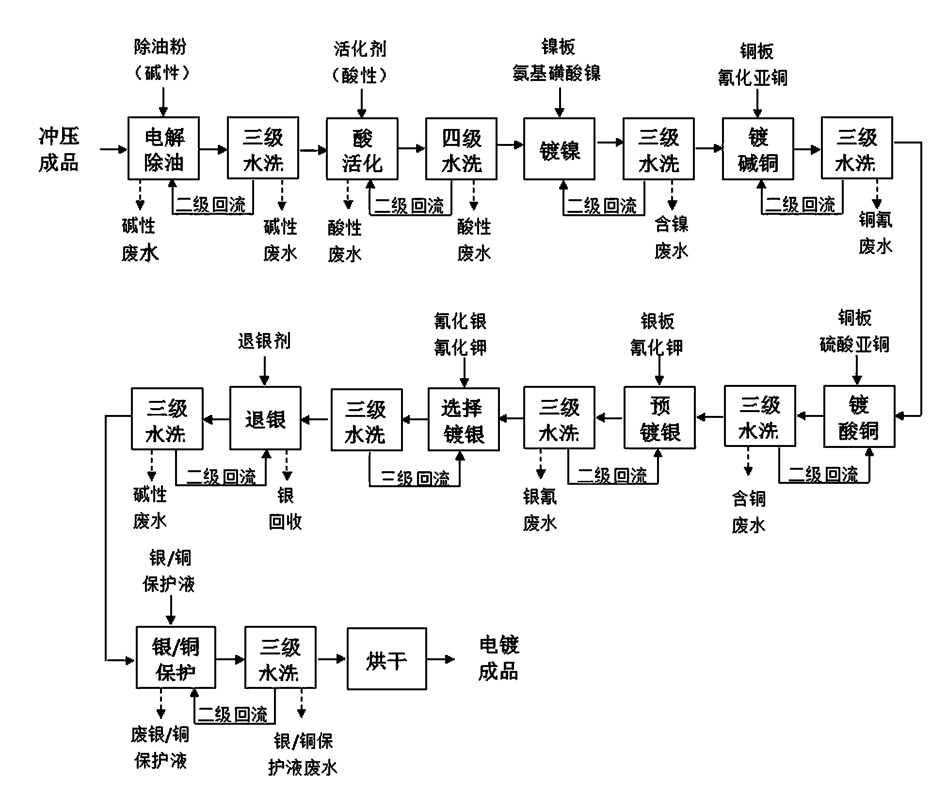
[0061] This embodiment provides a manufacturing process of a semiconductor lead frame, which is an improved process for manufacturing a semiconductor lead frame by the existing die stamping method, and the main improvement of the process lies in the surface treatment process.

[0062] like figure 1 As shown, this embodiment includes stamping, surface treatment and cutting forming. The specific process steps of surface treatment are: electrolytic degreasing, water washing, acid activation, water washing, nickel plating, water washing, alkali copper plating, water washing, acid copper plating, Water washing, pre-silvering, water washing, silver plating, water washing, desilvering, water washing, plating protection solution, water washing and drying.

[0063] The water washing step between the electrolytic degreasing step and the acid activation step is three-stage water washing, and the first two stages of water washing are refluxed to the electrolytic degreasing step;

[0064]...

Embodiment 2

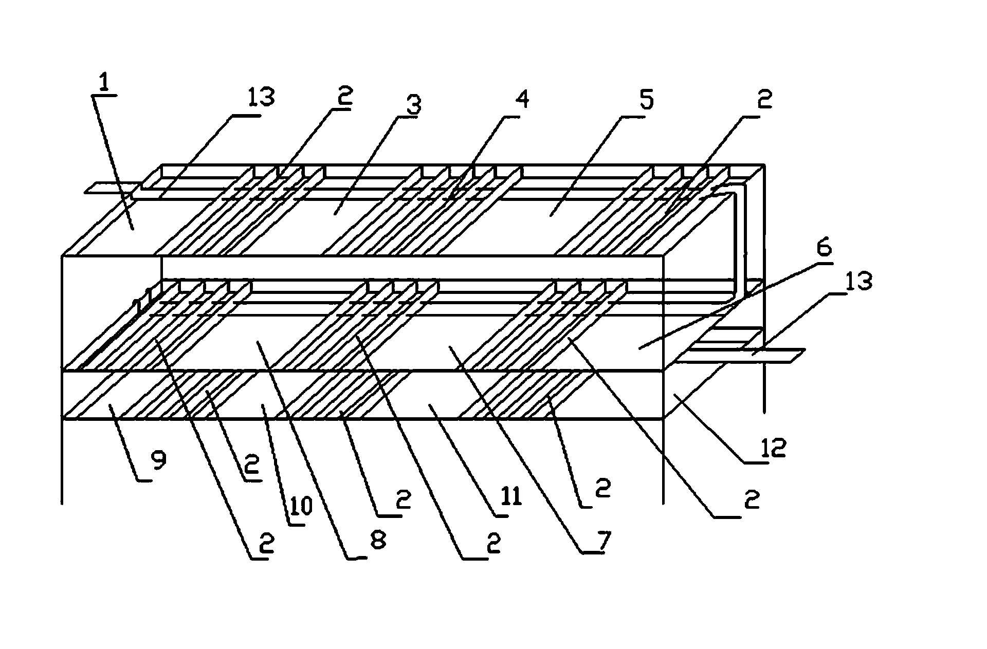
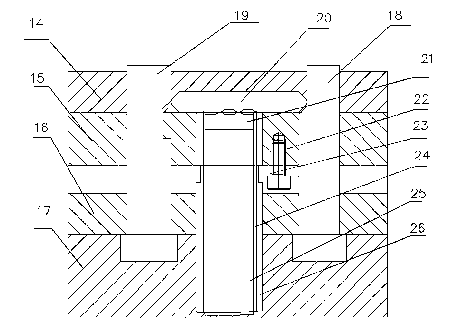
[0085] like Figure 3 to Figure 10 As shown, what this embodiment provides is a cutting and molding die for manufacturing semiconductor lead frames. This cutting and molding die combines the two processes of cutting and forming into one, and realizes these two processes on one mold, and at the same time does not The deformation of the semiconductor lead frame is caused, and the defect that the size of the semiconductor lead frame exceeds the standard error, that is, is out of tolerance, does not appear.

[0086] This cutting forming mold comprises upper mold, lower mold, cutting punch 25 and molding convex 26 molds, upper mold includes fixed backing plate 14 and fixing plate 15, and fixing backing plate 14 is positioned at the top of fixing plate 15, and lower mold includes unloading backing plate 16 and the unloading plate 17, the unloading backing plate 16 is located above the unloading plate 17, and is characterized in that: it also includes an upper slider 20, a lower slid...

Embodiment 3

[0097] In this implementation, the surface treatment process is the same as that of the embodiment, the cutting and forming mold is the same as that of the embodiment 2, and the others are the same as those of the prior art, and will not be repeated here.


PUM


Abstract

The invention relates to a semiconductor lead frame manufacturing technology which comprises the steps of stamping, surface treatment and cut-forming. The technology is characterized in that the surface treatment process specifically comprises the steps of electrolytic degreasing, washing, acid activation, washing, nickel plating, washing, alkaline copper plating, washing, acid copper plating, washing, silver preplating, washing, silver plating, silver removing, washing, protective solution plating, washing and drying. Plated layers of a semiconductor lead frame manufactured with the method are high in adhesive force and do not fall off easily. Meanwhile, the semiconductor lead frame is free of deformation and oversize, high in quality, and long in service life.

Description

technical field [0001] The invention relates to a manufacturing process for a semiconductor lead frame, in particular to a manufacturing process for manufacturing a semiconductor lead frame by using a mold stamping method. Background technique [0002] Semi-conductive lead frame refers to a thin metal frame used to connect the contact point of the chip inside the semiconductor integrated block and the external wire. Its production raw material is mainly copper coil. Conventional semiconductor lead frames mainly have two manufacturing processes, one is etching method, and the other is die stamping method. The etching method is to etch a part of the material with a chemical substance to make a product, which is mostly suitable for small-scale production; the die stamping method is made by stamping the thin plate material conveyed intermittently by the stamping force of the mold, and is mostly suitable for large-scale production. The mold stamping method generally has the foll...

Claims


Application Information

Patent Timeline
IPC IPC(8): H01L21/02H01L23/495C25D5/12
CPCH01L2924/0002H01L2924/00H01L21/4814C25D5/12H01L21/02068H01L23/49582
Inventor 黄斌任俊
Owner SICHUAN JINWAN ELECTRONICS
Why Eureka
Try Eureka