Fin-shaped semiconductor structure and forming method thereof
A semiconductor and fin-type technology, applied in the field of fin-type semiconductor structure and its formation, can solve problems such as high capacitance and large leakage current, and achieve the effects of improving sensitivity, prolonging service life, and improving device performance
- Summary
- Abstract
- Description
- Claims
- Application Information
AI Technical Summary
Problems solved by technology
Method used
Image

Examples
Embodiment 1
[0059] The present invention proposes a semiconductor structure and a manufacturing method thereof, such as Figure 1-17 Shown is a schematic diagram of the intermediate steps of the method. Hereinafter, each step of the embodiment of the present invention will be described in detail with reference to these figures.
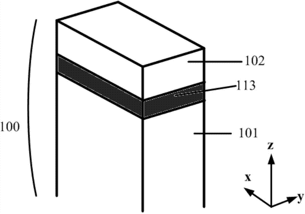
[0060] Step A: Provide a substrate 100 including a sacrificial region, and form a fin substrate 100 having a lower substrate 180 and a fin portion 110 on the substrate, the sacrificial region 113 is in the fin portion, refer to Figure 6 shown.
[0061] In the process of preparing the substrate, such as figure 1 As shown, a substrate 100 is provided, the substrate 100 includes a first substrate 101, the material of which can be silicon, and then a sacrificial region 113 is formed on the first substrate 101 by an epitaxy method. In an embodiment, the sacrificial region 113 is a sacrificial layer 113 that runs through the entire substrate. The material of the ...
Embodiment 2
[0090] Only the aspects of the second embodiment that differs from the first embodiment will be described below. Parts not described should be considered to be performed using the same steps, methods or processes as those in the first embodiment, so details will not be repeated here.
[0091] Step A: providing a substrate 100 including a sacrificial region 113 , forming a fin substrate 100 having a lower substrate 180 and a fin portion 110 on the substrate 100 , the sacrificial region 113 being in the fin portion.
[0092] Different from the first embodiment, in this embodiment, the sacrificial region 113 is not a sacrificial layer penetrating the fin portion, but a sacrificial block 113 .
[0093] The method of forming the sacrificial block 113 can be completed in the process of preparing the substrate 100. In this embodiment, a substrate 100 is provided, and a mask is formed at the position where the surface of the substrate 100 needs to be protected, so as to expose the par...
Embodiment 3
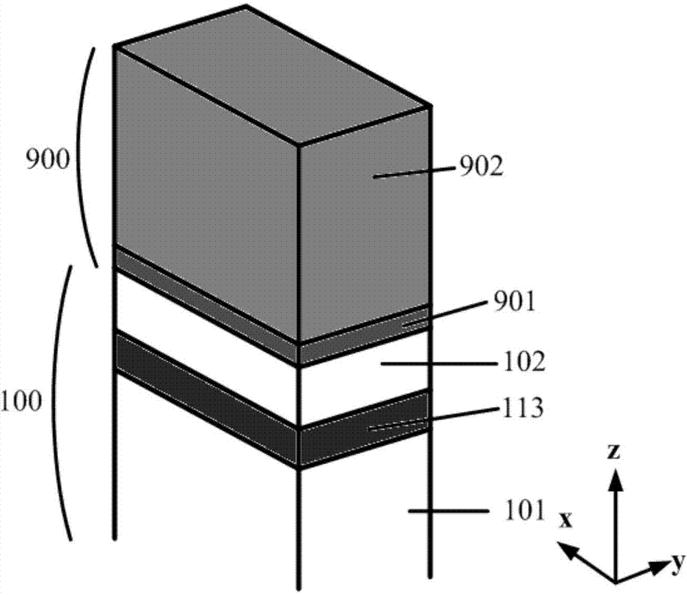
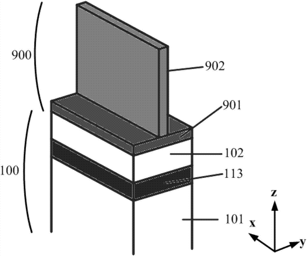
[0101] In addition, the present invention also proposes a fin-type semiconductor device structure, referring to Figure 14 The device has: a fin-shaped substrate 100 including a lower substrate 180 and a fin portion 110, a source region 6002 and a drain region 6001 on the fin portion 110, and the source region 6002 and the drain region 6001 span across the fin. The gate structure 410 on the portion 110, the fin portion below the gate structure is a channel, the shallow trench isolation 105 located on both sides of the fin portion 110 along the y direction and below the gate structure 410, the gate structure along the x direction 410 with sidewalls 500 on both sides, interlayer dielectric layers on both sides of the sidewalls 500 along the x direction, and the isolation region 300 formed in the fin portion 110 between the trench and the lower substrate. The fin part 110 may include an upper fin part 114 , a sacrificial region 113 and a lower fin part 112 . The width of the top...
PUM
 Abstract
Description
Claims
Application Information
 - R&D
- Intellectual Property
- Life Sciences
- Materials
- Tech Scout
- Unparalleled Data Quality
- Higher Quality Content
- 60% Fewer Hallucinations
Browse by: Latest US Patents, China's latest patents, Technical Efficacy Thesaurus, Application Domain, Technology Topic, Popular Technical Reports.
© 2025 PatSnap. All rights reserved.Legal|Privacy policy|Modern Slavery Act Transparency Statement|Sitemap|About US| Contact US: help@patsnap.com