Method for manufacturing gate oxide layer

A manufacturing method and gate oxide layer technology, applied in semiconductor/solid-state device manufacturing, electrical components, circuits, etc., can solve problems such as low nitrogen content and unstable nitrogen content, and achieve the effect of increasing nitrogen content

Inactive Publication Date: 2014-08-06
SHANGHAI HUALI MICROELECTRONICS CORP
View PDF4 Cites 12 Cited by
  • Summary
  • Abstract
  • Description
  • Claims
  • Application Information

AI Technical Summary

Problems solved by technology

[0009] The purpose of the present invention is to provide a method for manufacturing a gate oxide layer to so

Method used


Image

  • Method for manufacturing gate oxide layer

Examples


Embodiment Construction

[0027] The method for manufacturing the gate oxide layer proposed by the present invention will be further described in detail below with reference to the accompanying drawings and specific embodiments. Advantages and features of the present invention will be apparent from the following description and claims. It should be noted that all the drawings are in a very simplified form and use imprecise scales, and are only used to facilitate and clearly assist the purpose of illustrating the embodiments of the present invention.

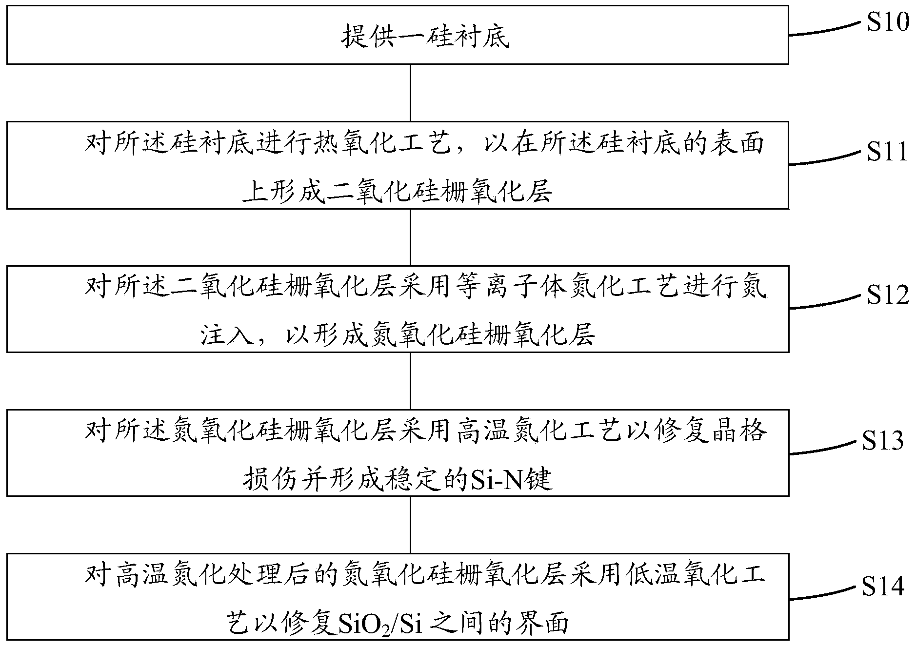
[0028] Please refer to figure 1 , which is a process flow diagram of a method for manufacturing a gate oxide layer according to an embodiment of the present invention. Such as figure 1 As shown, the manufacturing method of the gate oxide layer includes:

[0029] Step S10: providing a silicon substrate;

[0030] Step S11: performing a thermal oxidation process on the silicon substrate to form a silicon dioxide gate oxide layer on the surface of the sil...


PUM


Abstract

The invention provides a method for manufacturing a gate oxide layer. The method includes the steps of providing a silicon substrate, carrying out the thermal oxidation technology on the silicon substrate to form a silicon dioxide gate oxide layer on the surface of the silicon substrate, carrying out nitrogen injection on the silicon dioxide gate oxide layer with the plasma nitridation technology to form a silicon oxynitride gate oxide layer, carrying out the high-temperature nitridation technology on the silicon oxynitride gate oxide layer to repair crystal lattice damage and form stable Si-N bonds, and carrying out the low-temperature oxidation technology on the silicon oxynitride gate oxide layer after high-temperature nitridation processing is carried out to repair an interface between SiO2 and Si. By means of the method for manufacturing the gate oxide layer, the gate oxide layer after the nitrogen injection is processed with the high-temperature nitridation technology, the Si-N bonds of the silicon oxynitride gate oxide layer are stable, nitrogen atoms on the surface of the silicon oxynitride gate oxide layer are prevented from being continuously volatilized or diffused, and therefore the content of nitrogen in the gate oxide layer is effectively improved and kept stable.

Description

technical field [0001] The invention relates to the technical field of semiconductor manufacturing, in particular to a method for manufacturing a gate oxide layer. Background technique [0002] In semiconductor manufacturing technology, the gate oxide layer is usually used as a dielectric layer to achieve electrical isolation between the gate and the substrate. The performance of the gate oxide layer usually directly affects and determines the electrical characteristics and reliability of semiconductor devices. Therefore, the preparation process of the gate oxide layer is a key step in the semiconductor manufacturing process. [0003] As the feature size of semiconductor devices continues to shrink, the thickness of the gate oxide layer is getting thinner and thinner. As the gate oxide thickness decreases, gate leakage increases exponentially. On the other hand, there is a concentration gradient of impurities between the gate, the gate oxide layer and the silicon substrate...

Claims


Application Information

Patent Timeline
IPC IPC(8): H01L21/283
CPCH01L21/28202
Inventor 张红伟
Owner SHANGHAI HUALI MICROELECTRONICS CORP
Why Eureka
Try Eureka