Tunneling field-effect transistor capable of restraining nolinear opening of output and preparation method thereof

A tunneling field effect, transistor technology, applied in diodes, semiconductor devices, semiconductor/solid-state device manufacturing, etc., can solve problems such as large output resistance, achieve steep sub-threshold slopes, reduce production costs, and improve device output characteristics. Effect

Active Publication Date: 2014-08-13
PEKING UNIV
View PDF2 Cites 16 Cited by
  • Summary
  • Abstract
  • Description
  • Claims
  • Application Information

AI Technical Summary

Problems solved by technology

Therefore, the front part of the TFET output characteristic curve is a nonlinear curve exceeding the e index, that is, the nonlinear turn-on phenomenon of the output characteristic, which leads to a considerable output resistance of the device in circuit applications.

Method used


Image

  • Tunneling field-effect transistor capable of restraining nolinear opening of output and preparation method thereof
  • Tunneling field-effect transistor capable of restraining nolinear opening of output and preparation method thereof
  • Tunneling field-effect transistor capable of restraining nolinear opening of output and preparation method thereof

Examples


Embodiment Construction

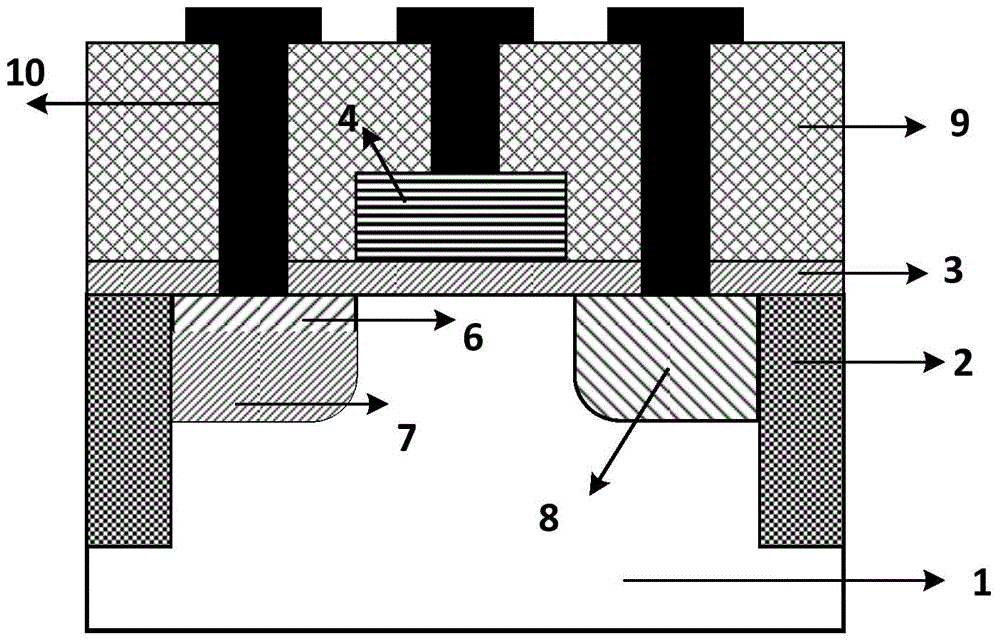
[0043] The implementation method of the tunneling field effect transistor for suppressing output nonlinear turn-on according to the present invention will be further described through specific embodiments below in conjunction with the accompanying drawings.

[0044] The specific implementation steps are as Figure 2-Figure 7 Shown: (This example takes N-type devices as an example, and P-type devices can be deduced by analogy)

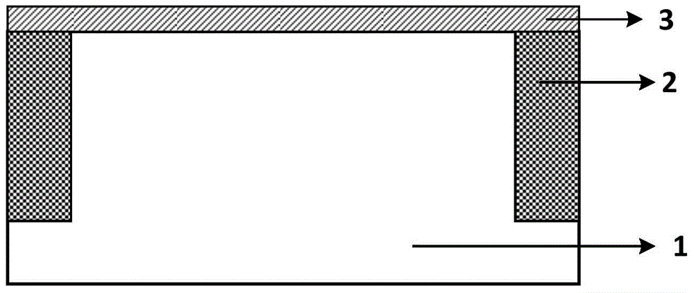
[0045] 1. The substrate doping concentration is lightly doped (about 1E13cm -3 -1E15cm -3 ), a layer of silicon dioxide is initially thermally oxidized on the InGaAs substrate 1 with a crystal orientation of , with a thickness of about 10 nm, and a layer of silicon nitride (Si 3 N 4 ), with a thickness of about 100nm, and then use shallow trench isolation technology to make STI isolation 2 in the active area, and then perform CMP, such as figure 2 shown.

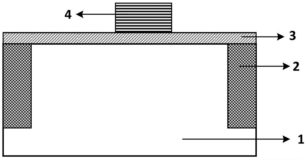
[0046] 2. Float away the silicon dioxide initially grown on the surface, and then thermally ...


PUM


Abstract

A tunneling field-effect transistor capable of restraining nolinear opening of output comprises a tunneling source region, a channel region, a drain region and a control grid positioned above a channel. The tunneling source region is III-V compound semiconductor mixed crystals, and a mixed crystal ratio of the mixed crystals gradually changes in the direction of the surface of a perpendicular device. An energy band structure of a heterogenous tunneling junction on the interface of the tunneling source region and the channel region gradually changes in the direction of the surface of the perpendicular device. A staggered-gap heterojunction tunneling source region is arranged on the surface of the device, and a tunneling junction on the surface of the device is a staggered-gap heterojunction. A broken-gap heterojunction tunneling source region is arranged at the position with a certain distance away from the surface of the device, and a tunneling junction at the position is a broken-gap heterojunction. The staggered-gap heterojunction tunneling source region and the broken-gap heterojunction tunneling source region have the same doping type. The tunneling field-effect transistor is simple in preparation process, a preparation method of the tunneling field-effect transistor is completely based on a standard CMOS IC process, the TFET device can be integrated in a CMOS integrated circuit effectively, a low-power-consumption integrated circuit composed of the TFET can be prepared through a standard process, therefore, production cost is reduced greatly, and the technological process is simplified.

Description

technical field [0001] The invention belongs to the field of field-effect transistor logic devices of CMOS ultra-large-scale integrated circuits (ULSI), and in particular relates to a tunneling field-effect transistor capable of suppressing output nonlinear turn-on and a preparation method thereof. Background technique [0002] Since the birth of integrated circuits, microelectronics integration technology has been developing continuously in accordance with "Moore's Law", and the size of semiconductor devices has been continuously reduced. As semiconductor devices enter the deep submicron range, traditional MOSFET devices are limited by the conduction mechanism of self-diffusion drift, and the subthreshold slope is limited by the thermoelectric potential kT / q, which cannot be reduced synchronously with the reduction of device size. As a result, the reduction of leakage current of MOSFET devices cannot meet the requirements of device size reduction, the energy consumption of ...

Claims


Application Information

Patent Timeline
Patent Type & Authority Applications(China)
IPC IPC(8): H01L29/739H01L29/06H01L21/331
CPCH01L29/0895H01L29/66356H01L29/7391
Inventor 黄如吴春蕾黄芊芊王佳鑫王阳元
Owner PEKING UNIV
Why Eureka
Try Eureka