Method for manufacturing flexible carbon nano-tube transistor

A technology of carbon nanotubes and single-walled carbon nanotubes, applied in transistors, nanotechnology, nanotechnology, etc., to achieve important application value, device performance improvement, and simplified process steps

Active Publication Date: 2014-08-20
SHANGHAI INTEGRATED CIRCUIT RES & DEV CENT
View PDF3 Cites 12 Cited by
  • Summary
  • Abstract
  • Description
  • Claims
  • Application Information

AI Technical Summary

Problems solved by technology

However, so far, the preparation of high-performance parallel array-based single-walled carbon nanotube transistors on flexible substrates has not been extensively studied. If parallel array-based single-walled carbon nanotubes ca...

Method used


Image

  • Method for manufacturing flexible carbon nano-tube transistor
  • Method for manufacturing flexible carbon nano-tube transistor
  • Method for manufacturing flexible carbon nano-tube transistor

Examples


preparation example Construction

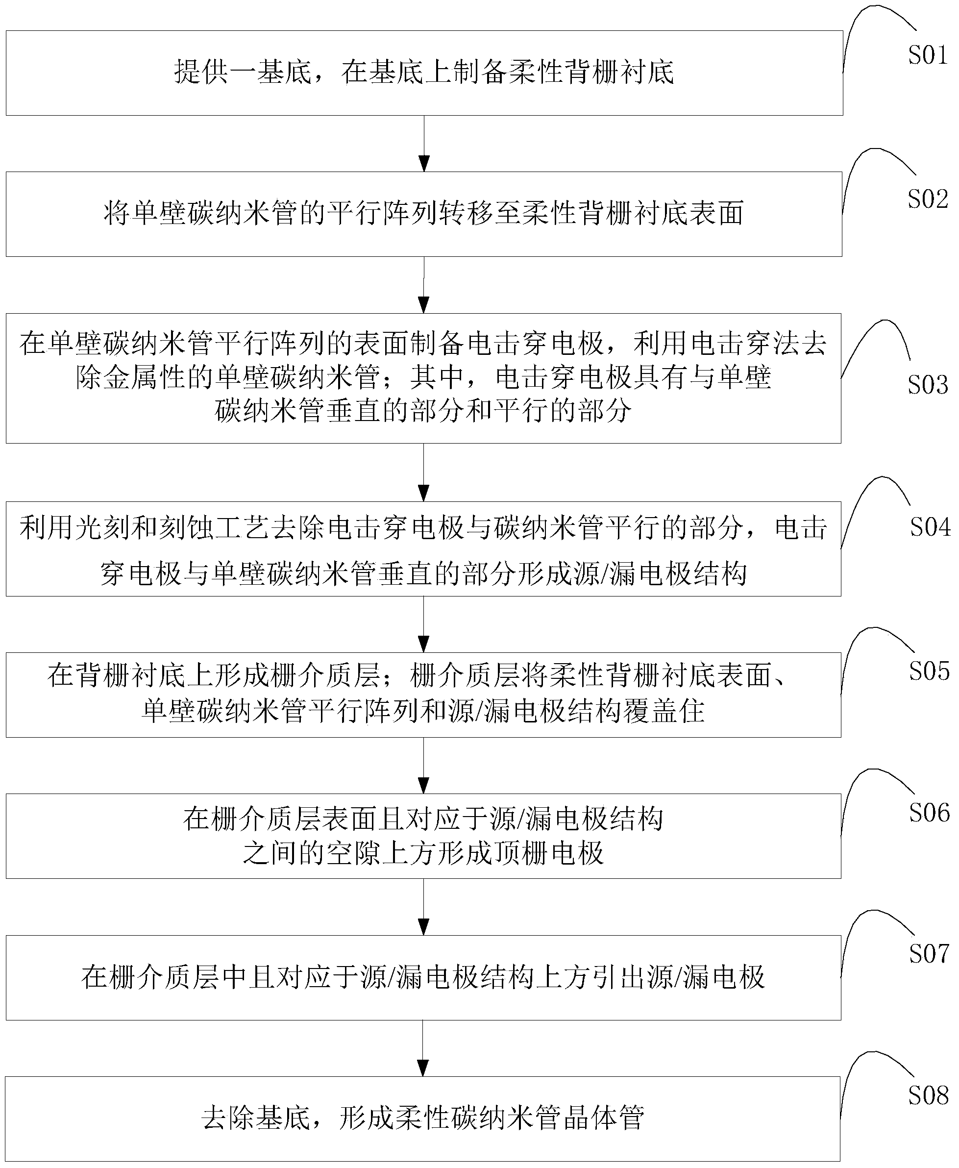
[0060] The preparation method of the flexible carbon nanotube transistor of the present invention comprises:

[0061] A substrate is provided, and a flexible backgate substrate is prepared on the substrate;

[0062] Transferring parallel arrays of single-walled carbon nanotubes to the surface of a back-gated substrate;

[0063] Prepare an electrical breakdown electrode on the surface of the single-walled carbon nanotube parallel array, and remove the metallic single-walled carbon nanotube by using the electrical breakdown method; wherein, the electrical breakdown electrode has a part parallel to the single-walled carbon nanotube and a vertical part ;

[0064] The part of the electrical breakdown electrode parallel to the single-walled carbon nanotube is removed by photolithography and etching process, and the part of the electrical breakdown electrode perpendicular to the carbon nanotube forms a source / drain electrode structure;

[0065] forming a gate dielectric layer on th...


PUM


Abstract

The invention provides a method for manufacturing a flexible carbon nano-tube transistor. The method comprises the following steps that a flexible back gate substrate is manufactured on a substrate; a single-wall carbon nano-tube parallel array is transferred to the surface of the flexible back gate substrate; metallic single-wall carbon nano-tubes are remoted through an electric breakdown method; a part of electric breakdown electrodes are removed through photoetching and etching processes, so that a source/drain electrode structure is formed; a gate dielectric layer is formed on the flexible back gate substrate; the surface of the flexible back gate substrate, the single-wall carbon nano-tube parallel array and source/drain electrode patterns are covered with the gate dielectric layer; top gate electrodes are formed on the surface of the gate dielectric layer; source/drain electrodes are led out of the source/drain electrode patterns; the substrate is removed, and the flexible carbon nano-tube transistor is formed. According to the method, the intrinsic characteristic that semiconductor single-wall carbon nano-tubes are high in migration rate is brought into full play, the electric breakdown electrodes are directly improved to be capable of serving as the following source/drain electrode structure, the process steps are simplified, and device performance is improved.

Description

technical field [0001] The invention relates to the technical field of semiconductors, in particular to a method for preparing a flexible carbon nanotube transistor. Background technique [0002] In recent years, with the rapid development of flexible display technology and smart wearable products, flexible electronics has received more and more attention, and research on flexible field-effect transistors (FETs) has gradually become a hot topic. The preparation process is mainly based on organic semiconductor materials, or adopts low-temperature polysilicon process. Although organic semiconductor materials have good flexibility and low process cost, their low carrier mobility greatly limits the improvement of device performance. At the same time, organic semiconductor materials are also extremely vulnerable to oxygen and humidity. , which leads to serious problems in the reliability of the device. Although the low-temperature polysilicon process can improve the reliability...

Claims


Application Information

Patent Timeline
IPC IPC(8): H01L21/336H01L21/28
CPCB82Y10/00H01L21/043H01L29/66045H01L29/775
Inventor 郭奥任铮胡少坚周伟
Owner SHANGHAI INTEGRATED CIRCUIT RES & DEV CENT
Why Eureka
Try Eureka