

Packaging process of flexible semiconductor film electronic device
A technology of electronic devices and packaging technology, which is applied in semiconductor/solid-state device manufacturing, semiconductor/solid-state device components, electrical components, etc., and can solve problems that affect device performance, increase production costs, and poor water-oxygen barrier performance
- Summary
- Abstract
- Description
- Claims
- Application Information
AI Technical Summary
Problems solved by technology
Method used
Image

Examples
Embodiment 1
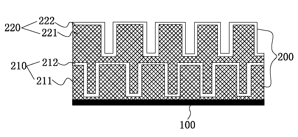
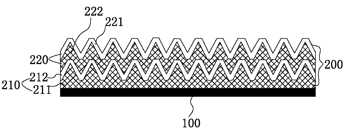
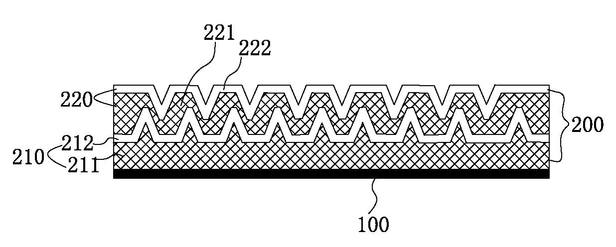
[0037] A packaging process for flexible semiconductor thin-film electronic devices, including the process of preparing a water-oxygen barrier layer. The water-oxygen barrier layer is formed by stacking one or more sets of water-oxygen barrier units, preferably two layers.
[0038] Each group of water and oxygen barrier units includes an organic barrier layer and an inorganic barrier layer. The surface of the organic barrier layer has an uneven structure, and the inorganic barrier layer is arranged on the upper surface of the organic barrier layer.
[0039] Due to the uneven surface structure of the organic barrier layer, the water-oxygen barrier unit composed of the inorganic barrier layer and the organic barrier layer can increase the scattering effect of water vapor and oxygen molecules when they diffuse in the organic film, and at the same time reduce the diffusion of water and oxygen molecules. Diffusion channels, thereby reducing the permeability of water and oxygen molecu...
Embodiment 2
[0045] A packaging process for flexible semiconductor thin-film electronic devices, other features are the same as in Embodiment 1, the difference is that an organic barrier layer is prepared by doping inorganic particles in a photoresist as a raw material, and the surface of the organic barrier layer has a Bubbles that are inflated by particles.
[0046] Wherein, the particle size of the inorganic particles doped in the photoresist is 0.01-10um, and the doping amount of the inorganic particles is 0.01g / mL-5g / mL. Preferably, the particle size of the inorganic particles doped in the photoresist is 2-5um, and the doping amount of the inorganic particles is 0.2g / mL.
[0047]In the invention, the bumps are formed on the surface of the organic barrier layer by doping the inorganic particles, so as to realize the formation of uneven topography on the surface of the organic barrier layer, and prepare the inorganic barrier layer on the surface of the organic barrier layer. By control...
Embodiment 3
[0049] A packaging process for a flexible semiconductor thin film electronic device, other features are the same as those of Embodiment 1 or 2, the difference is that: a base layer preparation process is also provided, that is, a base layer is prepared on the surface of the flexible semiconductor thin film electronic device to be packaged, and then A water and oxygen barrier layer is prepared on the base layer.
[0050] The material of the base layer can be Al 2 o 3 or Si 3 N 4 or SiO 2 And other inorganic materials, the thickness is usually 20~200nm. The base layer has good bonding performance with the device to be packaged, so that the water and oxygen barrier layer can be stably prepared on the base layer.
PUM
| Property | Measurement | Unit |
|---|---|---|
| Thickness | aaaaa | aaaaa |
| Particle size | aaaaa | aaaaa |
| Particle size | aaaaa | aaaaa |
Abstract
Description
Claims
Application Information