Interference filter, interference filter manufacturing method, optical module, electronic apparatus, and bonded substrate

An interference filter and manufacturing method technology, applied in chemical instruments and methods, optics, optical components, etc., can solve problems such as difficulty in ensuring surface accuracy, air leakage, and inability to fully ensure air tightness, and achieve high air tightness. , the effect of improving the bonding yield

Active Publication Date: 2014-09-17
SEIKO EPSON CORP
View PDF4 Cites 8 Cited by
  • Summary
  • Abstract
  • Description
  • Claims
  • Application Information

AI Technical Summary

Problems solved by technology

However, there is a problem that in these joints, in order to obtain good joint strength, high surface precision of the joint surface is required, and it is difficult to ensure the surface precision especially when the substrate is processed by etching or the like.
[0005] In addition, there are also problems such as insufficient airtightness, air leakage, etc.

Method used


Image

  • Interference filter, interference filter manufacturing method, optical module, electronic apparatus, and bonded substrate
  • Interference filter, interference filter manufacturing method, optical module, electronic apparatus, and bonded substrate
  • Interference filter, interference filter manufacturing method, optical module, electronic apparatus, and bonded substrate

Examples


no. 1 approach

[0092] Hereinafter, a first embodiment according to the present invention will be described with reference to the drawings.

[0093] The structure of the spectrometer

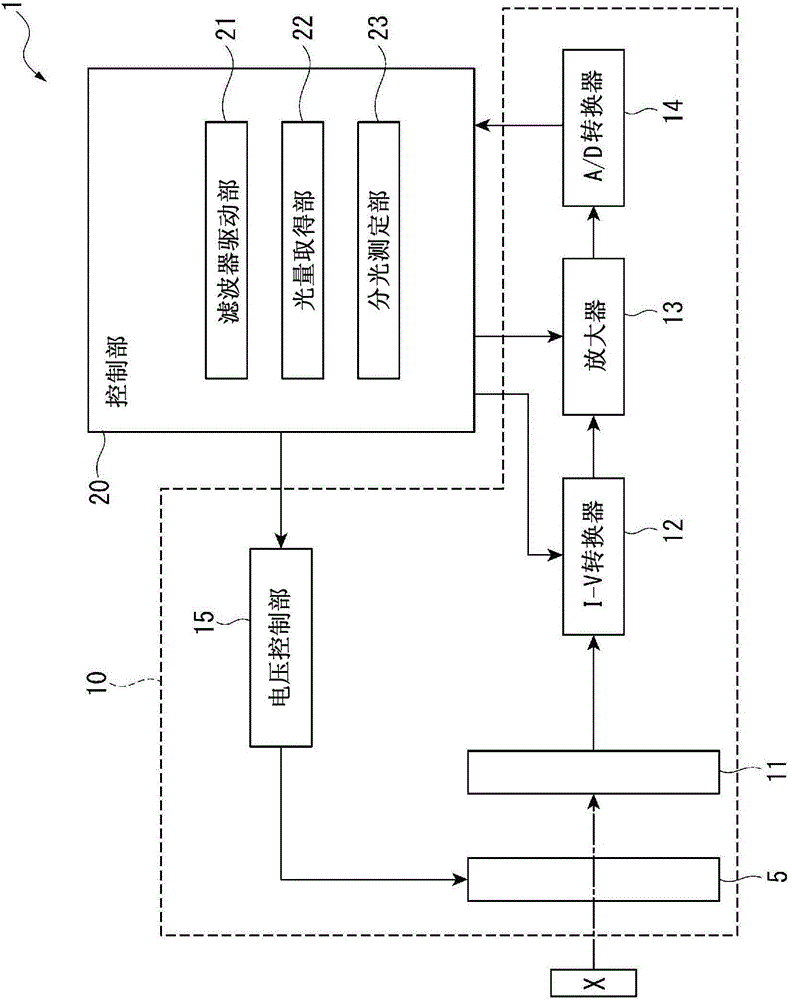
[0094] figure 1 It is a block diagram showing a schematic configuration of the spectrometry device according to the present invention.

[0095]The spectrometer 1 is an example of the electronic device of the present invention, and is a device that analyzes the light intensity of each wavelength of the measurement object light reflected by the measurement object X, and measures a spectral spectrum. In addition, in this embodiment, an example of measuring the measurement object light reflected by the measurement object X is shown. As the measurement object X, for example, when using a luminous body such as a liquid crystal panel, the light emitted by the luminous body can be used as the measurement object Light.

[0096] Next, if figure 1 As shown, this spectrometer 1 includes an optical module 10 and a contr...

no. 2 approach

[0250] Next, a second embodiment according to the present invention will be described with reference to the drawings.

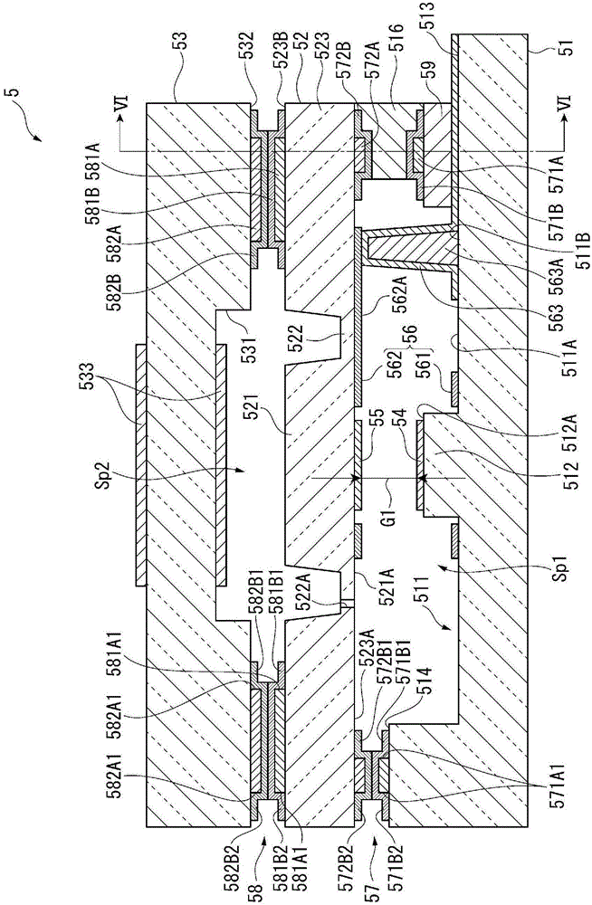
[0251] In the above-mentioned first embodiment, each of the surfaces to be joined 514, 523A, 523B, and 532 is shown as a flat surface, and the resin layers 571A, 572A, 581A, and 582A serving as base layers are formed on these surfaces to be joined 514, 523A, 523B, and 532. example of .

[0252] However, when the resin layers 571A, 572A, 581A, and 582A are formed, the edge 571A1 , 572A1 , 581A1 , and 582A1 may become thicker than other portions due to floating or the like. In this case, portions of the metal layers 571B, 572B, 581B, and 582B formed on the resin layers 571A, 572A, 581A, and 582A corresponding to the edges 571A1, 572A1, 581A1, and 582A1 also float up. Therefore, the metal layer 571B and the metal layer 572B, or the metal layer 581B and the metal layer 582B are in contact only in the floating portion, and the airtightness may not be sufficiently...

Embodiment approach

[0264] In addition, this invention is not limited to the above-mentioned embodiment, The deformation|transformation, improvement, etc. within the range which can achieve the objective of this invention are included in this invention.

[0265] For example, as the resin layer, as mentioned above, it is not limited to the plasma polymerized film, and may be made of other metal structures softer than the epoxy-based photosensitive material and the metal layer (Au). When an epoxy-based photosensitive material is used as the resin layer, since patterning with a photomask is possible, the accuracy of the formation position of the resin layer can be improved.

[0266] Moreover, although the structure which provided the resin layer 571A and the resin layer 572A as a base layer in the 1st junction part 57 is employ|adopted, it is not limited to this.

[0267] As the base layer, it may be provided on either one of the fixed substrate 51 and the movable substrate 52 . Therefore, for exam...


PUM


Abstract

A wavelength tunable interference filter includes a fixed substrate, a movable substrate, a fixed reflective film provided on the fixed substrate, a movable reflective film provided on the movable substrate so as to face the fixed reflective film, and a first bonding portion that bonds the fixed substrate and the movable substrate to each other. The first bonding portion includes a resin layer provided on the fixed substrate, a metal layer that is provided on the fixed substrate so as to cover the resin layer and that has smaller plasticity than the resin layer, and another metal layer that is provided on the movable substrate and that is bonded to the metal layer.

Description

technical field [0001] The present invention relates to an interference filter, a manufacturing method of the interference filter, an optical module, an electronic device, and a bonding substrate. Background technique [0002] In the prior art, there is known a spectroscopic filter that allows light of a specific wavelength to pass through by reflecting light between a pair of mirrors, and makes light of other wavelengths cancel each other through interference, thereby obtaining a specific value from the incident light. wavelength of light. Further, as such a spectroscopic filter, there is known a variable-wavelength interference filter that selects and emits emitted light by adjusting the distance between mirrors (for example, refer to Patent Document 1). [0003] The variable wavelength interference filter described in Patent Document 1 includes: a first glass substrate provided with a first reflective film; and a movable substrate bonded to the first glass substrate and ...

Claims


Application Information

Patent Timeline
Patent Type & Authority Applications(China)
IPC IPC(8): G02B26/00G02B5/28G01J3/28G01N21/25
CPCG02B26/001B32B37/0076B32B38/0008G02B5/28B81C3/001B81B3/00G01J3/26G01J3/51
Inventor 荒川克治
Owner SEIKO EPSON CORP
Why Eureka
Try Eureka