Packaging structure for integrating VCO and waveguide antenna

A packaging structure, waveguide antenna technology, applied in the direction of semiconductor devices, semiconductor/solid-state device parts, electrical components, etc., can solve the problems of restricting PCB circuit design and application, difficult to achieve impedance matching, increase design investment, etc., to achieve convenient Large-scale production and application, easy miniaturization design, and the effect of reducing difficulty

Inactive Publication Date: 2014-09-17
XIDIAN UNIV
View PDF4 Cites 9 Cited by
  • Summary
  • Abstract
  • Description
  • Claims
  • Application Information

AI Technical Summary

Problems solved by technology

[0004] At present, there are two main high-frequency packaging technologies on the market: (1) Four-sided flat no-lead package has been successfully applied in the frequency band below 40GHz, and the chips are interconnected with external circuits through gold wire bonding; Influenced by the parasitic effect of the wire bonding wire, it is difficult to achieve impedance matching and the insertion loss is large
The disadvantage of this method is that although it can work up to the E-band, its cost will be greatly increased due to the use of metal-ceramic packaging. In mass production, this disadvantage will be more prominent; and it cannot use standard production lines. When redesigning, it is necessary to overcome the influence of parasitic parameters between pads and pins on the overall performance of the chip, increase design investment, and also restrict later PCB circuit design and application

Method used


Image

  • Packaging structure for integrating VCO and waveguide antenna
  • Packaging structure for integrating VCO and waveguide antenna
  • Packaging structure for integrating VCO and waveguide antenna

Examples


Embodiment Construction

[0036] The present invention will be further described in detail below in conjunction with specific embodiments, which are explanations of the present invention rather than limitations.

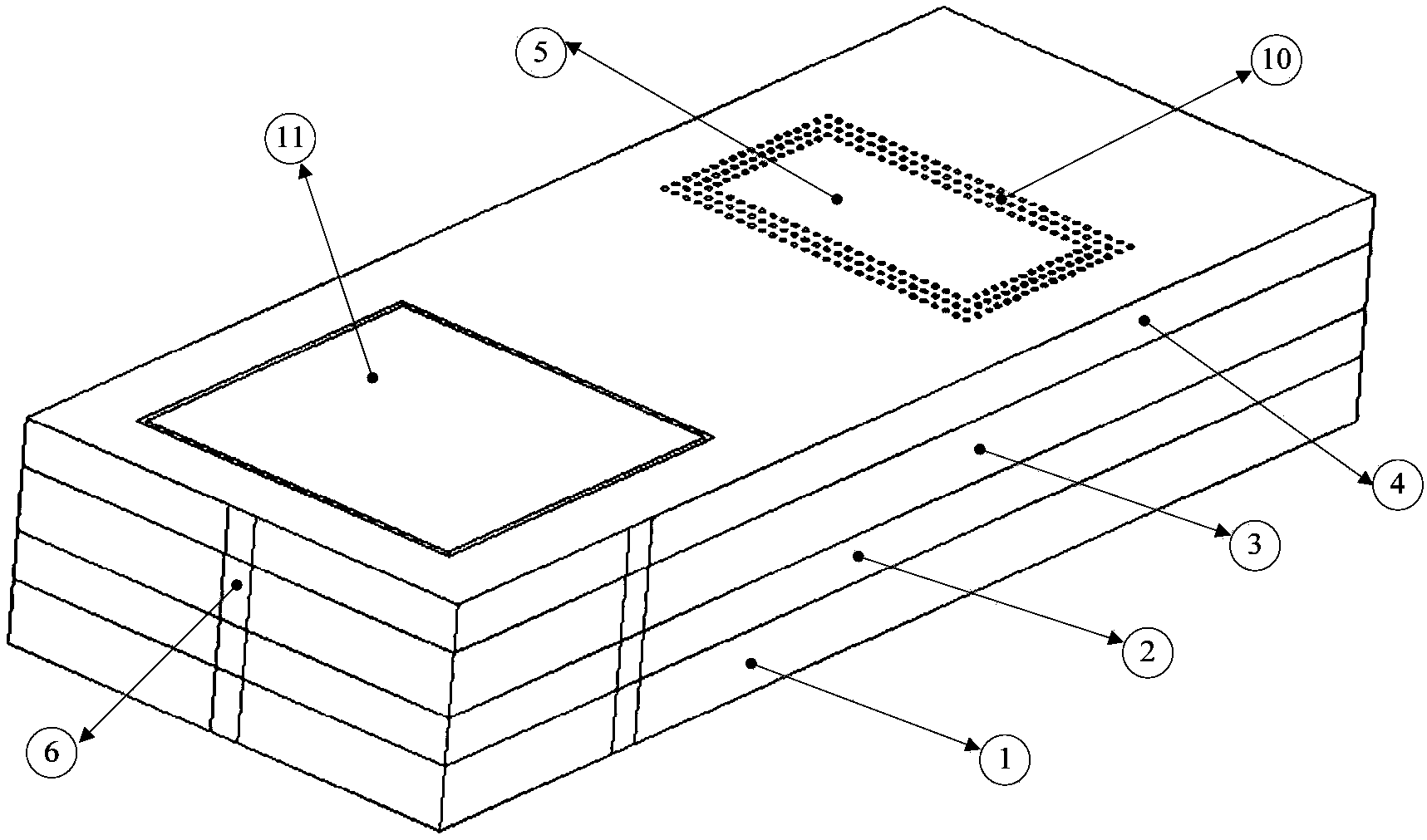
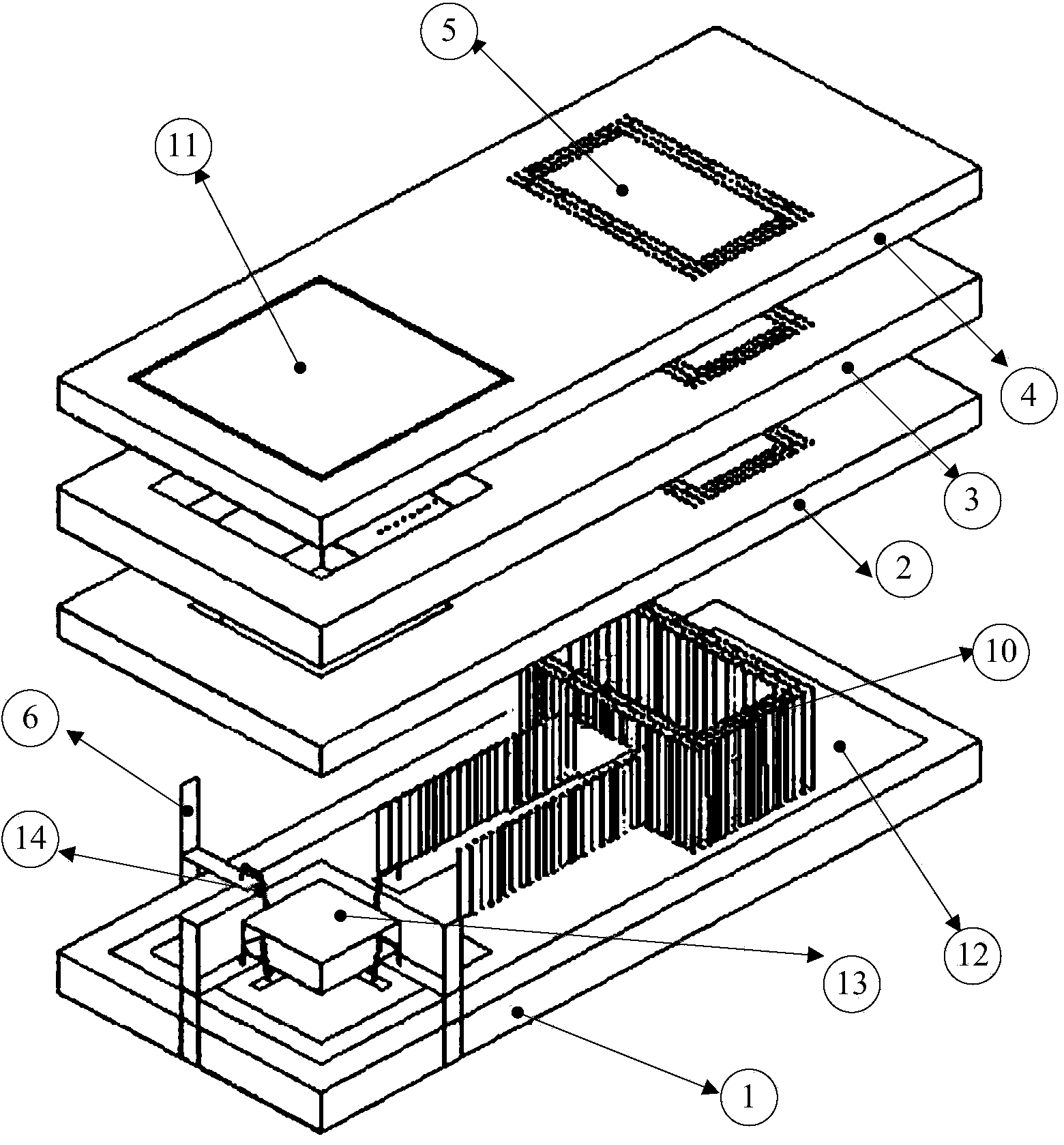
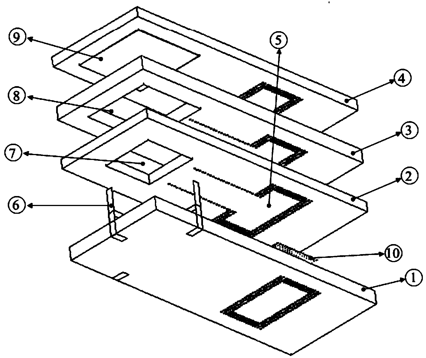
[0037] see Figure 1 ~ Figure 4 , a packaging structure integrating a VCO and a waveguide antenna, including an LTCC package composed of a bottom dielectric substrate layer, several intermediate dielectric substrate layers, and a top dielectric substrate layer. One end of the LTCC package is packaged with a VCO chip, and the other end is packaged with a waveguide reflection cavity. and microstrip coupled probes;

[0038] The VCO chip is arranged at one end of the bottom dielectric substrate layer, and the other end of the dielectric substrate layer is provided with a through hole matching the VCO chip, and the top dielectric substrate layer is also provided with a metal cover for sealing the through hole. The substrate layer is provided with a GND metal grid reflective surface that provides ...


PUM


Abstract

The invention discloses a packaging structure for integrating a VCO and a waveguide antenna. The packaging structure comprises an LTCC packaging body composed of a bottom dielectric substrate layer, a plurality of middle dielectric substrate layers and a top dielectric substrate layer. A VCO chip is packaged at one end of the LTCC packaging body, and a waveguide reflection cavity and a micro-strip coupling probe are packaged at the other end of the LTCC packaging body. Through the combination of the micro-strip waveguide conversion technology and the chip packaging technology, the E wave-band VCO and the micro-strip waveguide conversion antenna are integrated inside a standard LTCC packaging chip, the size for application and assembly of a microwave circuit is reduced, the miniaturization design of products is facilitated, and most importantly, the influence on the circuit by spurious and distribution parameters in the circuit connection process is effectively reduced. The performance of the packaging structure similar to that of a packaging mode through metal ceramic is obtained by the adoption of the LTCC packaging technology, the working frequency relative bandwidth is larger than 20 percent, and insertion losses caused by micro-strip waveguide conversion are smaller than 1.2 dB within the working band.

Description

technical field [0001] The invention belongs to the technical field of E-band chip packaging, and relates to a packaging structure integrating a VCO and a waveguide antenna. Background technique [0002] E-band (60GHz-90GHz) is receiving more and more attention due to low frequency, crowded spectrum and the pursuit of better performance. At present, many countries in Europe are gradually increasing investment in the development of E-band microwave electronic components, but the technical difficulty of their design and installation is high, and the contradiction between performance and cost has always been the main factor restricting their more commercial applications. However, due to a series of demands in the market, a more reliable and stable way is needed to reduce the cost of the product, simplify the application method and expand the scope of application to achieve its wide application in various fields. With the surface mount technology (SMT ) mature application, prov...

Claims


Application Information

Patent Timeline
IPC IPC(8): H01L23/58
Inventor 侯建强张江涛苟仲荣霍云峰王黎莹史凯运雷永亮闫耀峰张玉赵勋旺
Owner XIDIAN UNIV
Why Eureka
Try Eureka