Z-source high-gain low-switching-stress direct current boost converter

A switching stress and DC boost technology, which is applied in the direction of converting DC power input to DC power output, output power conversion devices, instruments, etc., can solve the problems that are difficult to achieve high efficiency, small size, low noise, and low cost, and achieve shortening The effects of on-time, simple circuit topology, and low cost

Inactive Publication Date: 2014-09-17
SHANGHAI UNIVERSITY OF ELECTRIC POWER
View PDF5 Cites 7 Cited by
  • Summary
  • Abstract
  • Description
  • Claims
  • Application Information

AI Technical Summary

Problems solved by technology

In view of the above reasons, it is difficult for traditional step-up DC converters to achieve the goals of high efficiency, small size, low noise and low cost

Method used


Image

  • Z-source high-gain low-switching-stress direct current boost converter
  • Z-source high-gain low-switching-stress direct current boost converter
  • Z-source high-gain low-switching-stress direct current boost converter

Examples


Embodiment Construction

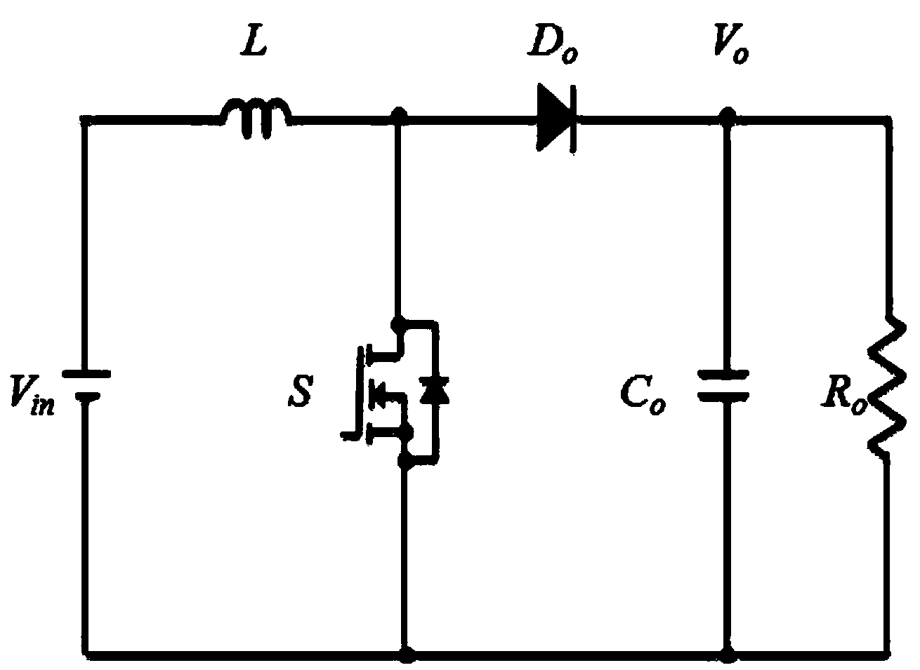
[0019] Such as figure 1 As shown in the topology diagram of the traditional boost DC converter, the positive pole of the input power supply passes through the inductor L, and then one way passes through the MOSFET switch tube to return to the negative pole of the input power supply, and the other way passes through the freewheeling diode D in turn. o , filter capacitor C o Back to the negative pole of the input power supply, the load R o in parallel with the filter capacitor C o ends.

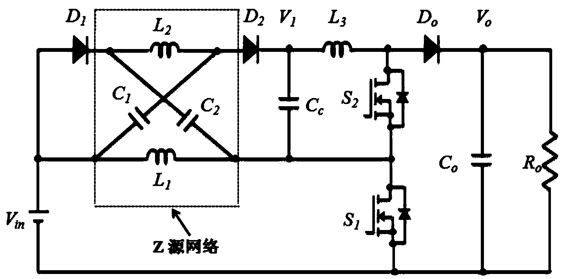
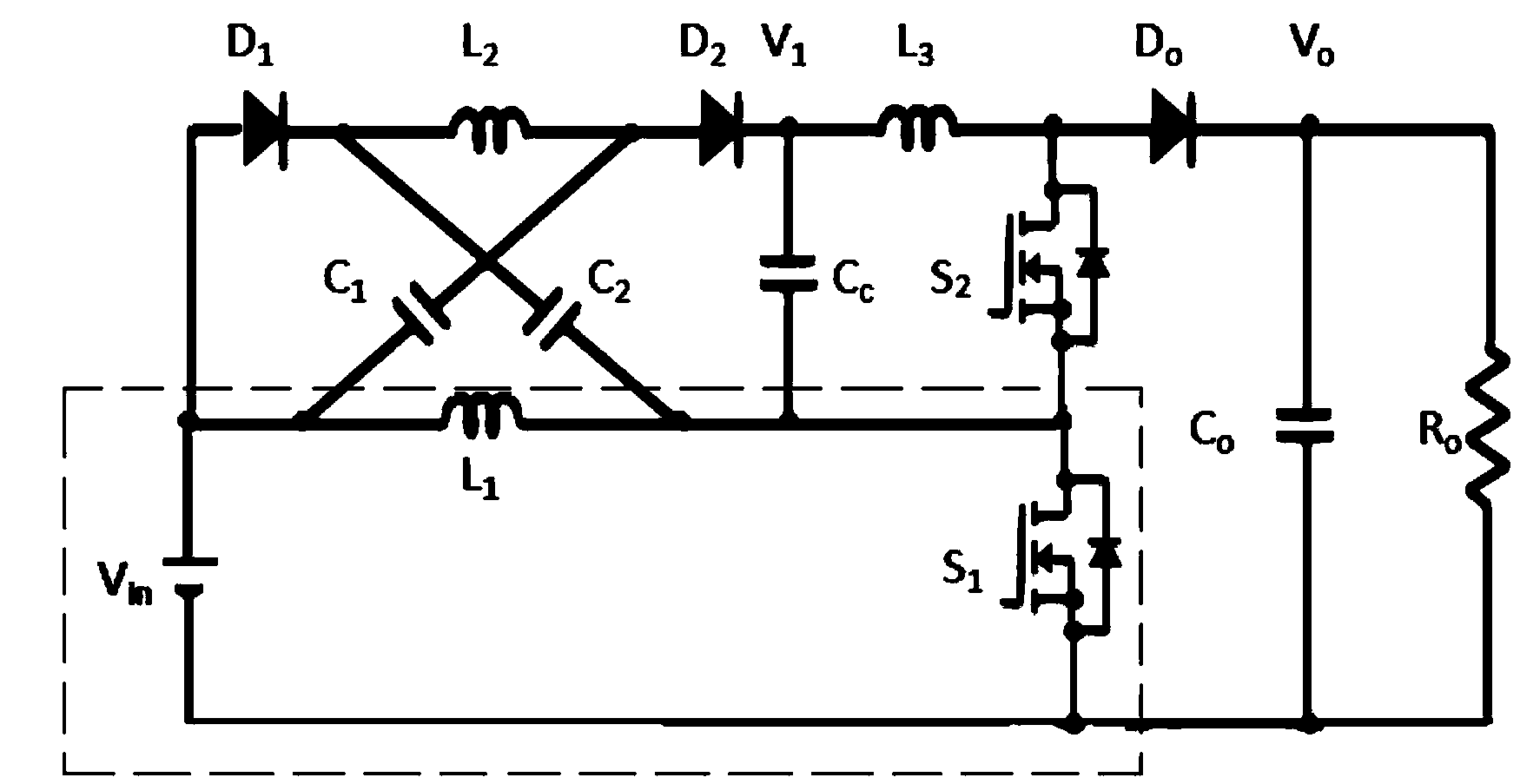
[0020] figure 2 The topological structure diagram of the step-up DC converter with high gain and low switching stress of the Z source of the present invention is shown. One of the positive poles of the input power supply is directly connected to the input of the Z source, and the other is passed through the diode D 1 Enter the Z source; the output of the Z source passes through the diode D 2 Divided into two routes, one route passes through the clamping capacitor C c Connect to MOSFET sw...


PUM


Abstract

The invention relates to a Z-source high-gain low-switching-stress direct current boost converter. On the basis of a traditional boost direct-current converter topological structure, a novel circuit topological structure is achieved by adopting a mode that an X-type Z-source network, a simple inductor and a simple capacitor are connected in series and parallel. The Z-source high-gain low-switching-stress direct current boost converter can obtain high voltage conversion gain and further reduce voltage stresses exerted onto two ends of a master switch, and a development target of enabling the direct current boost converter to be efficient, small in size and low in noise and cost is effectively achieved. Under the condition of low duty ratio, high gain is achieved. Due to the fact that the breakover time of the master switch is shortened, a peak value of input current is effectively reduced, and breakover consumption is reduced. The voltage stress of a switch tube is reduced from (i)Vo( / i) to (i)Vo( / i) / 3, 2(i)Vo( / i) / 3, and the hardware manufacturing cost is reduced. A transformer, a coupling inductor and a multistage connecting mode are not needed, and a circuit topological structure is simple. The target of enabling the direct current boost converter to be efficient, small in size and low in noise and cost can be achieved.

Description

technical field [0001] The invention relates to a DC boost converter, in particular to a Z-source high-gain DC boost converter with low switch stress. Background technique [0002] In recent years, the research on the development and utilization of new energy has become more and more extensive and in-depth at home and abroad, especially the research on photovoltaic power generation systems. my country's photovoltaic industry is developing rapidly, and its market share ranks among the top in the world. However, the output voltage of a single photovoltaic panel is low, and it is difficult to meet the requirements of the DC bus voltage of the subsequent inverter. Requirements see 1. Li Xuebin, Zhao Caihong, Huang Xiaohua, Application of cascaded converters in superconducting energy storage systems [J]. Power Grid Technology, 2006, 30(16): 54-58; 2. Fang Yu, Ma Xudong, Topology Analysis of a New Coupled Inductor Dual Boost Photovoltaic Micro-inverter[J]. Automation of Electric...

Claims


Application Information

Patent Timeline
Patent Type & Authority Applications(China)
IPC IPC(8): H02M3/155
Inventor 赵晋斌梁晓霞屈克庆
Owner SHANGHAI UNIVERSITY OF ELECTRIC POWER
Why Eureka
Try Eureka