PCB (printed circuit board) layout design method reducing differential crosstalk

A design method and differential line technology, applied in computing, special data processing applications, instruments, etc., can solve the problems of increasing crosstalk voltage, affecting product design quality, and large noise voltage amplitude, etc., achieving good use value and simple structure , Improve the effect of product quality

Inactive Publication Date: 2014-10-15
LANGCHAO ELECTRONIC INFORMATION IND CO LTD
View PDF0 Cites 8 Cited by
  • Summary
  • Abstract
  • Description
  • Claims
  • Application Information

AI Technical Summary

Problems solved by technology

Therefore, the influence of crosstalk is introduced, and the improvement of signal speed and the reduction of the coupling space of differential paths will inevitably aggravate the substantial increase of crosstalk voltage, which will affect the design quality of products
[0003] In the traditional differential pair wiring, because no consideration is given to how the wiring can reduce noise, the order of the differential lines that are terminated or drawn from the differential pads of the chip is very random.
That is to say: it is common to encounter a Step pulse excitation on the differential attack line, and it is found through simulation that the noise at the far end is a bit large; this differential wiring method will generate a large noise voltage amplitude at the far end of the signal (that is, the signal receiving end)

Method used


Image

  • PCB (printed circuit board) layout design method reducing differential crosstalk

Examples


Embodiment Construction

[0009] A PCB routing design method for reducing differential crosstalk according to the present invention will be described in detail below in conjunction with the accompanying drawings.

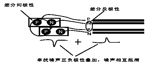
[0010] Such as figure 1 As shown, a PCB routing design method for reducing differential crosstalk of the present invention, in its structure, when the chip differential pin pad and the differential pair layout are coupled and routed, the coupling polarity of the chip pin and the coupling polarity of the differential line pair In this way, when the noise signals are superimposed, due to the opposite amplitude polarity, most of the noise energy is bound to superimpose and cancel each other, so the crosstalk noise can be effectively reduced.

[0011] At present, there are two types of chip differential pin pads and differential pair layout coupling routing modes, namely, the same phase mode and the phase reverse mode. Among them, the phase direction of the differential pair means that in the t...


PUM


Abstract

The invention provides a PCB layout design method reducing differential crosstalk. When a chip differential pin bonding pan and a differential pair perform coupling layout, chip pins and the differential pair are in opposite coupling polarity, and crosstalk noises correspondingly generated by the chip pins and the differential pair are in opposite polarity, so that when noise signals are superpositioned, due to the opposite amplitude polarity, most of noise energy is bound to offset due to mutual superposition, and further crosstalk noise can be effectively reduced. Compared with the prior art, the PCB layout design method reduces signal crosstalk by optimizing the layout mode, thereby improving the product quality and effectively reducing the crosstalk influence due to high-density interconnection of high-frequency signals. Meanwhile, the PCB layout design method reducing the differential crosstalk has the advantages of being reasonable in design, simple in structure, convenient to use and the like, thereby obtaining high usage values.

Description

technical field [0001] The invention relates to the field of computer PCB main board design, in particular to a PCB routing design method for reducing differential crosstalk. Background technique [0002] Due to the parasitic inductance and capacitance effect on the signal propagation path when laying out the PCB main board, when the signal propagates on a PCB Trace path, it will inevitably propagate to other adjacent ones through the coupled parasitic inductance and capacitance. Trace, and generate voltage noise on the near end and far end of the Trace. Therefore, the influence of crosstalk is introduced, and the improvement of signal speed and the reduction of the coupling space of the differential path will inevitably aggravate the substantial increase of crosstalk voltage, thereby affecting the design quality of the product. [0003] In traditional differential pair wiring, because no consideration is given to how to better reduce noise, the order of the differential li...

Claims


Application Information

Patent Timeline
Patent Type & Authority Applications(China)
IPC IPC(8): G06F17/50
Inventor 武宁吴福宽
Owner LANGCHAO ELECTRONIC INFORMATION IND CO LTD
Why Eureka
Try Eureka