Electronic module and manufacturing method thereof

A technology of electronic modules and electronic components, which is applied in semiconductor/solid-state device manufacturing, circuits, electrical components, etc., can solve problems affecting the characteristics of electronic components, reducing performance, and failure of electronic components, achieving both heat dissipation effect and increased surface area Effect

Active Publication Date: 2014-10-15
UNIVERSAL SCIENTIFIC INDUSTRIAL (SHANGHAI) CO LTD +1
View PDF1 Cites 2 Cited by
  • Summary
  • Abstract
  • Description
  • Claims
  • Application Information

AI Technical Summary

Problems solved by technology

Because the coefficient of thermal expansion of metal is much larger than that of epoxy resin, when the circuit board is heated during assembly, it is easy to cause the problem of de-lamination
[0006] Furthermore, due to the epoxy resin film sandwiched between the metal and the metal, a capacitor-like structure is formed, which may also affect the characteristics of the original electronic components
Moreover, the capacitive effect of coupling caused by the metal layer close to the active component will make the electronic component fail or degrade the performance

Method used


Image

  • Electronic module and manufacturing method thereof
  • Electronic module and manufacturing method thereof
  • Electronic module and manufacturing method thereof

Examples


Embodiment Construction

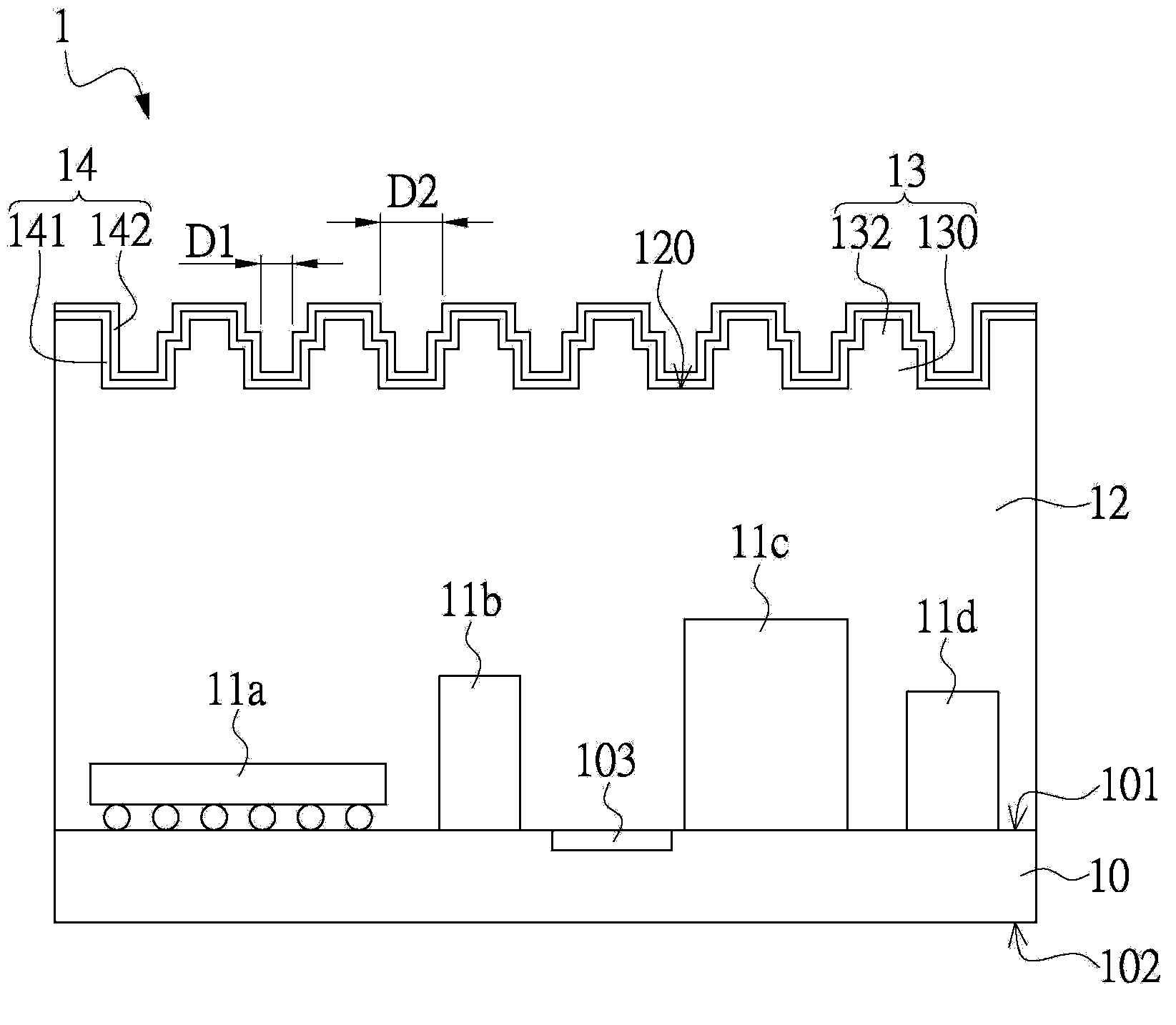
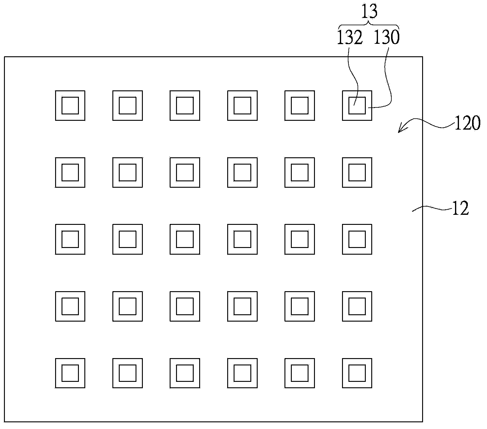
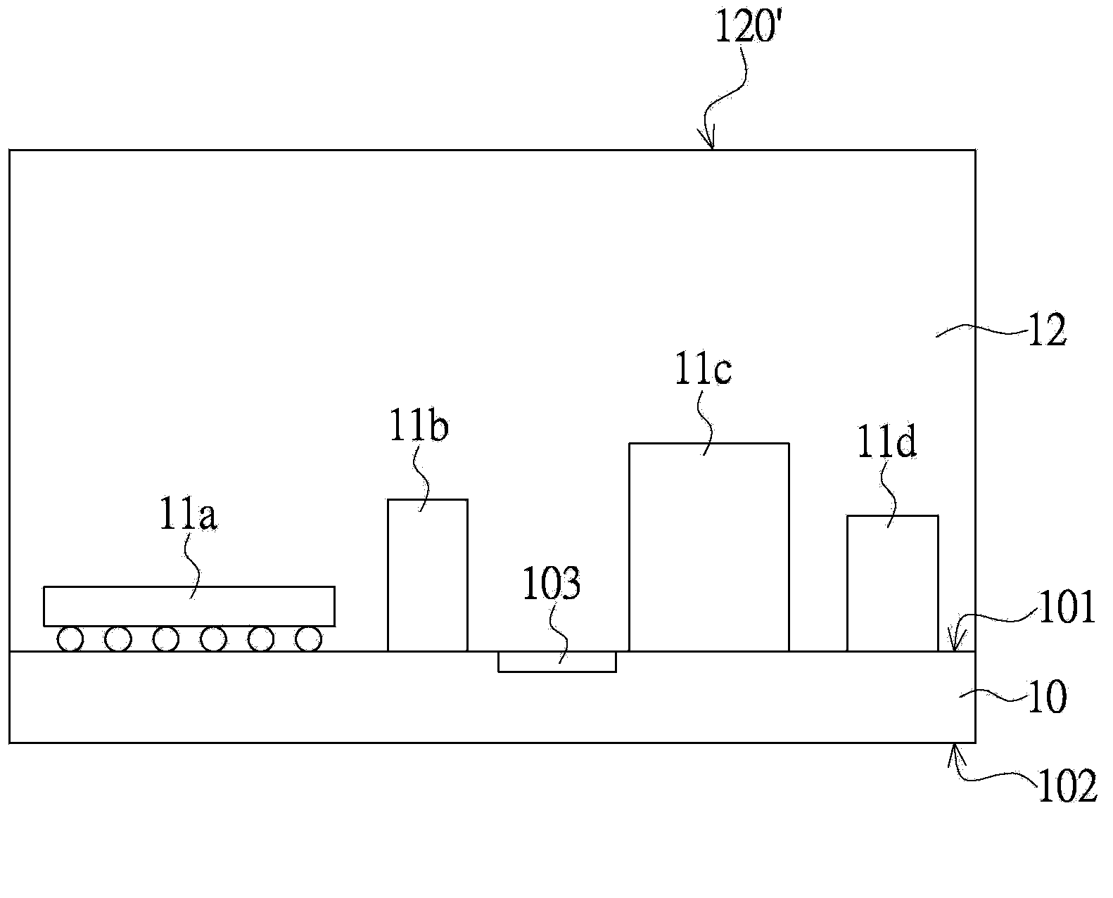
[0040] Please refer to figure 1 . figure 1 A cutaway side view of an electronic module according to an embodiment of the present invention is shown. The electronic module 1 includes a substrate 10 , electronic components 11 a - 11 d , a molding layer 12 and a composite electromagnetic wave shielding layer 14 .

[0041] The substrate 10 has a carrying surface 101 and a bottom surface 102 . The substrate 10 also has a plurality of preset pads 103 and circuit layers (not shown). The pad 103 is made of conductive material, such as copper, to be electrically connected to a conductive circuit (not shown) or a ground plane (not shown). Wherein, the pads 103 and the circuit layer (not shown) are located on the substrate 10 or buried in the substrate 10 . The material of the substrate 10 can vary according to the process and product requirements. For example, the semiconductor industry is a silicon-containing semiconductor wafer, and in other applications, it can be a PCB substrate...


PUM


Abstract

The invention discloses an electronic module and a manufacturing method thereof. The electronic module comprises a substrate, an electronic element, a mould sealing layer and a composite electromagnetic wave mask layer. The electronic element is configured on the substrate. The mould sealing layer covers a part of bearing surface of the electronic element and the substrate. The mould sealing layer is provided with an upper surface which is provided with a three-dimensional geometric pattern. The composite electromagnetic wave mask layer covers the upper surface of the mould sealing layer with the advantage of the form so that electromagnetic wave is shielded. The composite electromagnetic wave mask layer comprises a magnetic material layer and a conductive material layer.

Description

technical field [0001] The present invention relates to an electronic module, in particular to an electronic module with an electromagnetic wave shielding structure. Background technique [0002] Most of today's electronic products, such as smart phones, laptop computers or tablet computers, etc., are developing towards the goals of miniaturization, thinning, multi-function and high speed. In order to meet the demands of the market, electronic components in electronic products need to be reduced accordingly, and at the same time, they need to have higher operating frequencies. Due to the high distribution density of electronic components, the distance between the signal transmission lines between electronic components is getting closer, and the electronic components need to operate at a high operating frequency, so that electromagnetic radiation from the outside of electronic products or internal electronic components The mutual electromagnetic interference situation is als...

Claims


Application Information

Patent Timeline
IPC IPC(8): H01L23/552H01L21/56
CPCH01L2924/1815H01L2224/16225H01L2924/3025
Inventor 陈仁君张欣晴
Owner UNIVERSAL SCIENTIFIC INDUSTRIAL (SHANGHAI) CO LTD
Why Eureka
Try Eureka