Method for improving reliability of gate oxide layer of peripheral circuit area of flash memory

A flash memory, peripheral circuit area technology, applied in circuits, electrical components, semiconductor devices, etc., can solve the problems of reduced gate oxide integrity and uniformity, reduced gate oxide reliability, and device doping profile offset. , resulting in improved reliability, ease of implementation, increased integrity and uniformity

Active Publication Date: 2014-10-22
SEMICON MFG INT (SHANGHAI) CORP
View PDF6 Cites 3 Cited by
  • Summary
  • Abstract
  • Description
  • Claims
  • Application Information

AI Technical Summary

Problems solved by technology

[0005] However, while nitriding the tunnel oxide layer to improve the reliability of the memory cell region, a nitrogen-containing region is also formed on the top of the semiconductor substrate in the peripheral circuit region of the flash memory.
And because the Si-N bond of this nitrogen-containing region is not easy to break, the nitrogen-containing region at the top of the semiconductor substrate cannot be easily removed by conventional methods.
The existence of the nitrogen-containing region inhibits the growth of the gate oxide layer of the MOS device on the surface of the semiconductor substrate in the peripheral circuit area, so that the thickness of the formed gate oxide layer is insufficient. When the gate of the MOS device is loaded with high voltage, the thinner gate The oxide layer is easily broken down, which reduces the reliability of the gate oxide layer. Furthermore, compared with the flat semiconductor substrate surface, the gate oxide layer formed on the semiconductor substrate at the corner of the isolation structure is thinner, The integrity and uniformity of the gate oxide layer are reduced, resulting in the local electric field enhancement of the gate oxide layer of the MOS device at the corner of the isolation structure (local electric field enhancement), which directly causes the failure of the MOS device of the semiconductor substrate in the peripheral circuit area
[0006] Further, in the prior art, when removing the nitrogen-containing region on the top of the semiconductor substrate located in the peripheral circuit area, the oxidation treatment is carried out by means of furnace tube oxidation (reoxidation), but the high temperature of the furnace tube (often exceeding 800°C) will produce The additional thermal budget not only increases the fabrication cost, but also shifts the doping profile of the device

Method used


Image

  • Method for improving reliability of gate oxide layer of peripheral circuit area of flash memory
  • Method for improving reliability of gate oxide layer of peripheral circuit area of flash memory
  • Method for improving reliability of gate oxide layer of peripheral circuit area of flash memory

Examples


Embodiment 1

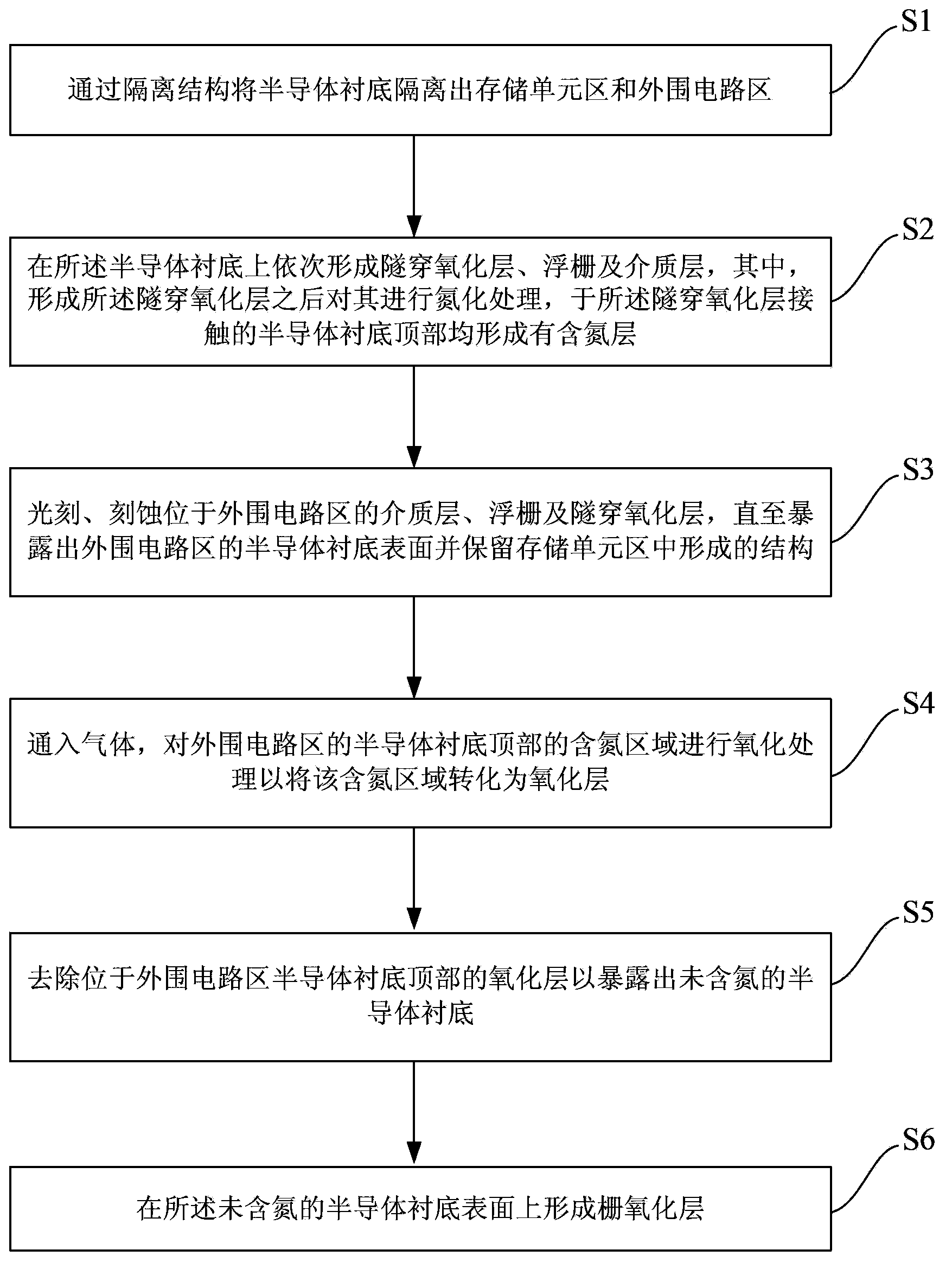
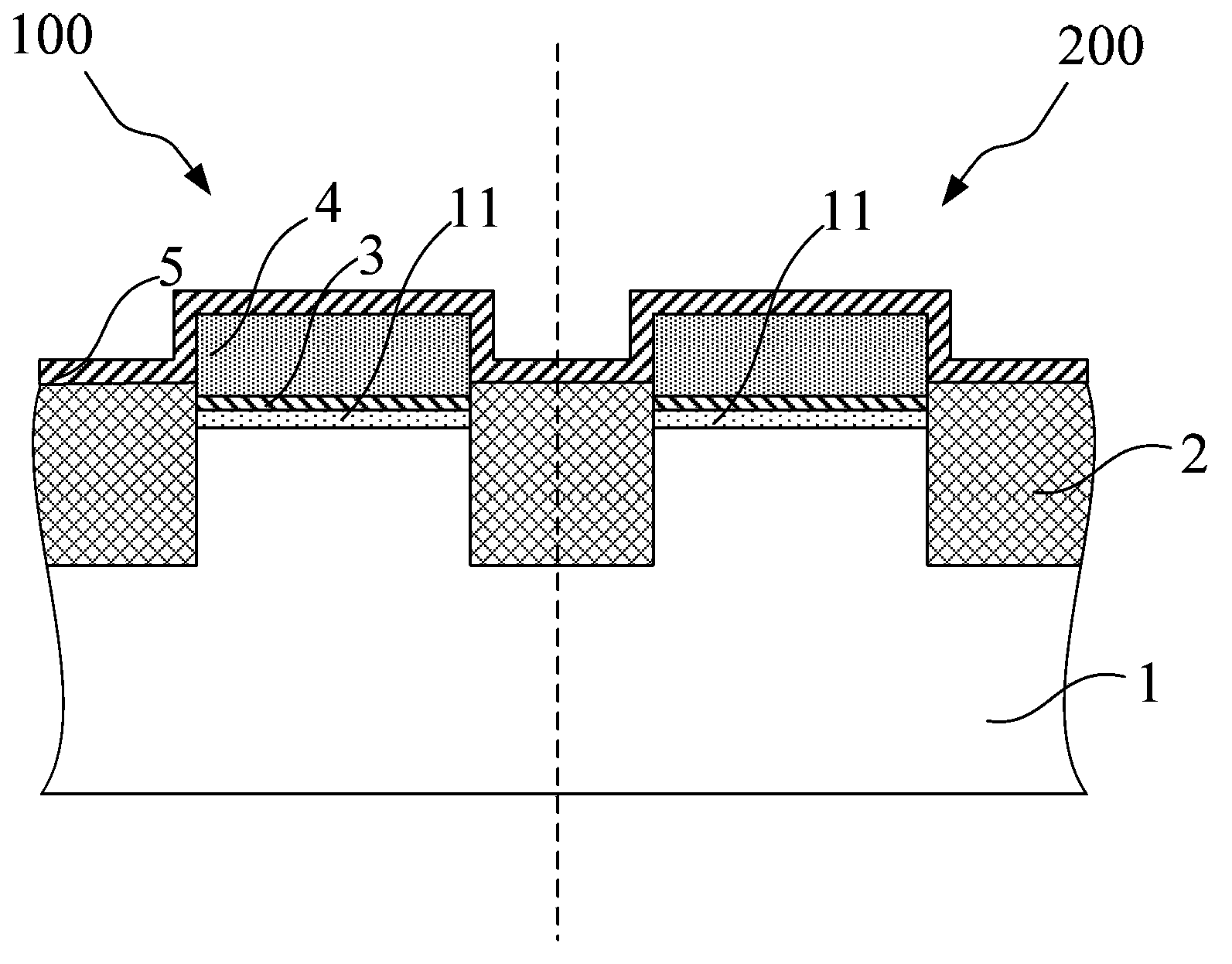
[0041] Such as Figure 1 to Figure 6 As shown, the present invention provides a method for improving the reliability of the gate oxide layer in the peripheral circuit region of the flash memory, and the method at least includes the following steps:

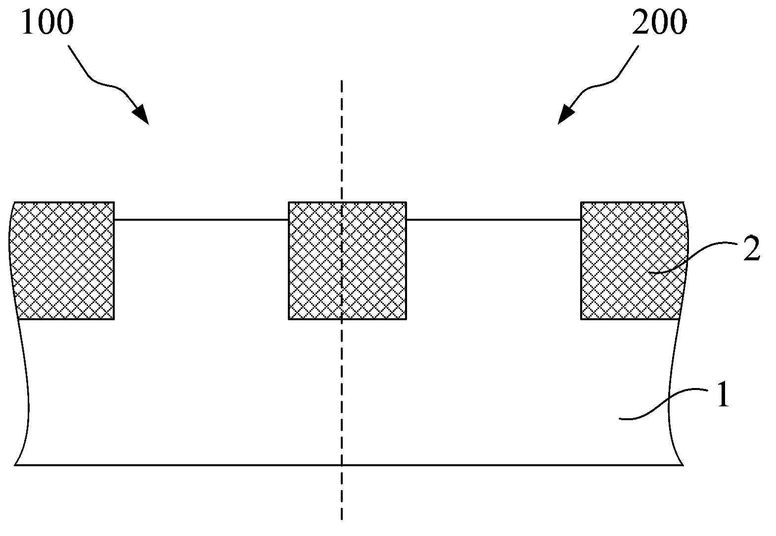
[0042] Do step 1) first, see figure 1 In step S1 and figure 2 , provide a semiconductor substrate 1 , and isolate the semiconductor substrate 1 from the memory cell region 100 and the peripheral circuit region 200 through the isolation structure 2 .

[0043] It should be pointed out that the specific steps of preparing shallow trench isolation 2 are: etching isolation trenches arranged in parallel on the semiconductor substrate formed with a hard mask, and then filling and planarizing the isolation trenches to achieve forming shallow trench isolation, wherein the surface of the shallow trench isolation is on the same plane as the surface of the hard mask on the semiconductor substrate, and then removing the hard mask to form ...

Embodiment 2

[0059]The scheme of embodiment 2 is basically the same as that of embodiment 1, the difference is only the gas introduced in step 4) and the relevant process conditions of oxidation treatment. For the rest of the same steps, please refer to the relevant description of embodiment 1, which will not be repeated here Let me repeat them one by one.

[0060] Firstly execute step 1) to step 3), please refer to the first embodiment for details. Then go to step 4).

[0061] In step 4) of Example 2, under the temperature condition of 100~150°C, H 2 SO 4 with H 2 o 2 The mixture (sulfuric peroxide mixture, SPM) gas is used to oxidize the nitrogen-containing region 11 on the top of the semiconductor substrate 1 in the peripheral circuit region 200 to convert the nitrogen-containing region 11 into an oxide layer 7 . Among them, H 2 SO 4 with H 2 o 2 The concentration ratio ranges from 5:1 to 7:1, and the thickness of the oxide layer is 50-100 angstroms. In the second embodiment, ...


PUM

PropertyMeasurementUnit
Thicknessaaaaaaaaaa
Thicknessaaaaaaaaaa

Abstract

The invention provides a method for improving the reliability of a gate oxide layer of a peripheral circuit area of a flash memory. The method includes the following steps that: oxidation treatment is performed on a nitrogen containing region of the top of a semiconductor substrate at the peripheral circuit area; and the nitrogen containing region is converted into an oxide layer, and the oxide layer is removed, and therefore, a nitrogen-free semiconductor substrate surface of the peripheral circuit area is exposed; and a gate oxide layer is grown on the nitrogen-free semiconductor substrate surface. With the method adopted, when an MOS device is manufactured in the peripheral circuit area in a subsequent process, the nitrogen containing region of the top of the semiconductor substrate is removed, and therefore, the growth difficulty of the gate oxide layer on the surface of the semiconductor substrate can be lowered, and especially, the growth capacity of the gate oxide layer on the semiconductor substrate at corners of an isolation structure can be improved, and the integrity and uniformity of gate oxide layer growth can be increased, and the reliability of the gate oxide layer of the MOS device can be improved; and the oxidation treatment mentioned in the invention is performed at room temperature or low temperature, and therefore, thermal budget in the prior art can be decreased, and device doping profile shift can be avoided. The method is advantageous in convenient implementation and simple operation.

Description

technical field [0001] The invention belongs to the field of manufacturing technology of semiconductor devices, and relates to a method for manufacturing a gate oxide layer, in particular to a method for improving the reliability of the gate oxide layer in the peripheral circuit area of ​​a flash memory memory. Background technique [0002] Flash memory (flash memory, referred to as flash memory) is a programmable erasable, non-volatile (non-volatile) memory, that is, it can save information content even when there is no external power supply, which makes the device itself do not need to waste power In terms of data storage, flash memory also has the characteristics of repeated reading and writing, small size, high capacity, and portability, which makes flash memory especially suitable for use in portable devices, and has become one of the mainstream research in the industry. [0003] A typical flash memory is mainly composed of a floating gate (Floating Gate) used to store ...

Claims


Application Information

Patent Timeline
IPC IPC(8): H01L21/28
CPCH01L29/42364
Inventor 王成诚李绍彬杨芸
Owner SEMICON MFG INT (SHANGHAI) CORP
Why Eureka
Try Eureka