Aluminum-based circuit board and preparation method thereof, and full packaging electronic component

A technology for aluminum-based circuit boards and electronic components, which is applied to printed circuits connected to non-printed electrical components, removing conductive materials by chemical/electrolytic methods, and printed circuit components, etc. Poor strength, difficulty in roughening the alumina layer, etc., to achieve the effect of simplifying the process, overcoming the difficulty in roughening or being easily damaged by corrosion, and maintaining a stable structure

Active Publication Date: 2014-10-22
MIDEA GRP CO LTD
View PDF6 Cites 5 Cited by
  • Summary
  • Abstract
  • Description
  • Claims
  • Application Information

AI Technical Summary

Problems solved by technology

[0005] Based on this, it is necessary to provide an aluminum-based circuit board for the preparation of fully packaged electronic components in view of the difficulties in coarsening the aluminum oxide layer of the traditional aluminum substrate and the poor bonding strength between the aluminum substrate and the molding compound.

Method used


Image

  • Aluminum-based circuit board and preparation method thereof, and full packaging electronic component
  • Aluminum-based circuit board and preparation method thereof, and full packaging electronic component
  • Aluminum-based circuit board and preparation method thereof, and full packaging electronic component

Examples


preparation example Construction

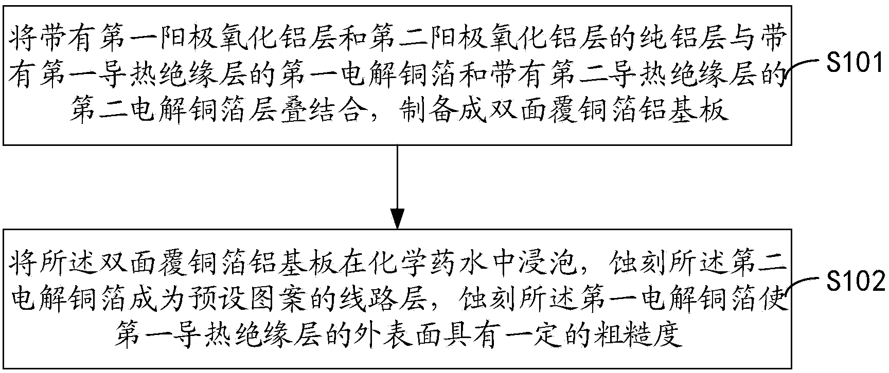
[0024] Correspondingly. The invention also provides a method for preparing an aluminum-based circuit board for preparing fully packaged electronic components with simple procedures and high production efficiency. This method can be used to prepare the above as figure 1 Shown aluminum base circuit board 1, the technique of this method is as image 3 shown, please also refer to figure 2 , which includes the following steps:

[0025] Step S101. Combine the pure aluminum layer 13 with the first anodized aluminum layer 12 and the second anodized aluminum layer 14 with the first electrolytic copper foil with the first thermally conductive insulating layer 11 and the second thermally conductive insulating layer 15 The second electrolytic copper foil is laminated and combined to prepare a double-sided copper-clad aluminum substrate;

[0026] Step S102. Soak the double-sided copper-clad aluminum substrate in chemical liquid, etch the second electrolytic copper foil combined with t...

Embodiment 1

[0045] An aluminum-based circuit board 1 for fully-packaged electronic components, a fully-packaged electronic component, and a preparation method for fully-packaged electronic components.

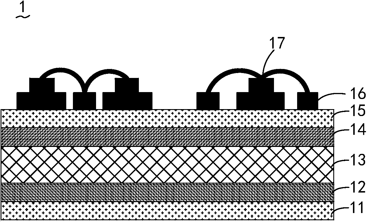
[0046] The structure of the aluminum base circuit board 1 is as follows: figure 1 As shown, it includes a first thermally conductive insulating layer 11, a first anodized aluminum layer 12, a pure aluminum layer 13, a second anodized aluminum layer 14, a second thermally conductive insulating layer 15 and a circuit layer that are sequentially stacked and combined 16 and electronic components 17 soldered on the circuit layer 16. Wherein, the thickness of the first thermally conductive insulating layer 11 is 75 μm, see Example 1 in Table 1 below.

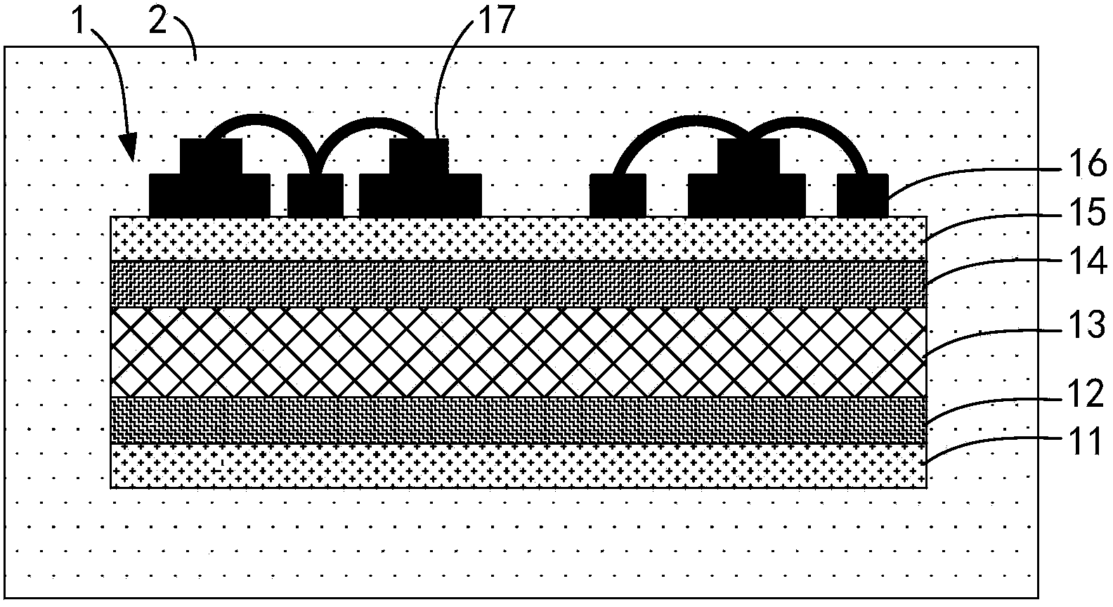
[0047] The fully encapsulated electronic components such as figure 2 As shown, its structure includes an aluminum-based circuit board 1 and an encapsulation layer 2 that fully encapsulates the aluminum-based circuit board.

[0048] The above-m...

Embodiment 2

[0053] An aluminum-based circuit board 1 for fully-packaged electronic components, a fully-packaged electronic component, and a preparation method for fully-packaged electronic components.

[0054] The structures of the aluminum-based circuit board 1 and the fully packaged electronic components are the same as those of the aluminum-based circuit board and the fully packaged electronic components in Embodiment 1. The difference is that the thickness of the first thermally conductive insulating layer 11 is 100 μm, see Example 2 in Table 1 below.

[0055] Refer to Example 1 for the above aluminum-based circuit board 1 and the preparation method of the fully packaged electronic components.


PUM


Abstract

Provided is an aluminum-based circuit board and a preparation method thereof, and a full packaging electronic component. The aluminum-based circuit board is used for preparing the full packaging electronic component, and comprises a first heat-conducting insulating layer, a first anode aluminum oxide layer, a pure aluminum layer, a second anode aluminum oxide layer, a second heat-conducting insulating layer and a line layer which are laminated and combined in turn. The first heat-conducting insulating layer is provided with a rough external surface. The first heat-conducting insulating layer is formed via an electrolytic copper foil etched by chemical liquid medicine so that the external surface of the first heat-conducting insulating layer has certain roughness, bonding strength between the aluminum-based circuit board and a packaging layer of the electronic component is substantially enhanced, and the structure of the aforementioned full packaging electronic component comprising the aluminum-based circuit board is enabled to be stable without de-lamination or cracking. Besides, heat radiation of the full packaging electronic component is also substantially enhanced by high bonding strength so that integrated reliability of the full packaging electronic component is enhanced.

Description

technical field [0001] The invention belongs to the technical field of electronic devices, and in particular relates to an aluminum-based circuit board used for preparing a fully packaged electronic component, a preparation method thereof, and a fully packaged electronic component. Background technique [0002] The intelligent power module (IPM) generates a lot of heat, so a good heat dissipation design is required to solve the reliability problem. A common practice in the industry is to install a heat sink on the package and expose the heat sink, which is a semi-encapsulated structure. At present, metal-based circuit boards are widely used as insulation and heat dissipation components for power devices. These circuit boards generally consist of a three-layer structure of metal substrates, insulating layers, and copper foils, and most of them are cheap and lightweight aluminum substrates. [0003] Traditional semi-encapsulated power modules are not highly integrated, so peri...

Claims


Application Information

Patent Timeline
Patent Type & Authority Applications(China)
IPC IPC(8): H05K1/02H05K3/06H05K1/18
Inventor 王新雷
Owner MIDEA GRP CO LTD
Why Eureka
Try Eureka