

A method for balancing stress on dbc board and dbc board packaging structure
A stress and balance technology, applied in electrical components, electrical solid devices, circuits, etc., can solve the problems of large idle space of DBC board 12, small number of chips 11, warping of DBC board 12, etc., to improve performance and aesthetics, The effect of reducing production costs and reducing warpage
- Summary
- Abstract
- Description
- Claims
- Application Information
AI Technical Summary
Problems solved by technology
Method used
Image

Examples
Embodiment 1
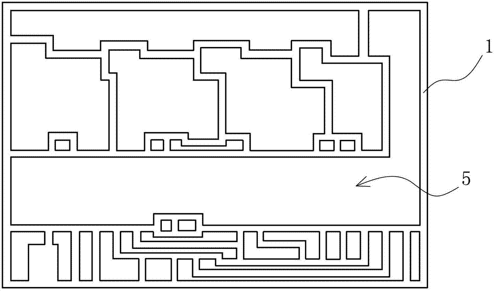
[0028] Embodiment one: see Figure 3-4 As shown, a method for balancing stress on a DBC board and a packaging structure of a DBC board, components are pasted on a DBC board 1 with etched lines, and the pasted components include four chips 2, four accessories 3 and three Metal dummy 4, after pasting the chip 2 and accessories 3 according to the design layout, the idle space 5 left on the DBC board 1 is pasted with the metal dummy 4, so that the components pasted on the DBC board 1 Uniform distribution for uniform thermal stress. The above-mentioned metal dummy is a thin metal sheet made of metal material, which replaces the position of the chip, and is powered on but does not have the function of the chip. The purpose is to balance the thermal stress of the DBC board.
[0029] Such as image 3 As shown, in this embodiment, the metal dummy sheet 4 is a solder paste sheet, which is produced during the DBC board solder paste printing process. The idle space 5 is obtained by red...
Embodiment 2
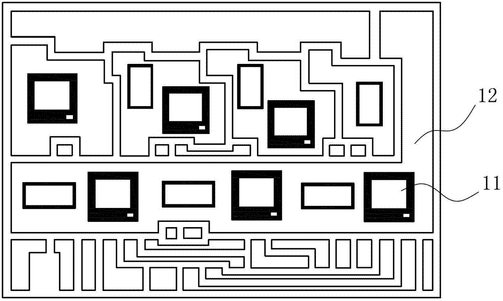
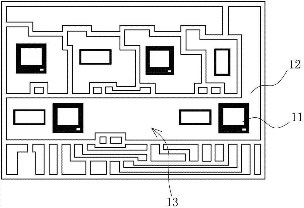
[0031] Embodiment two: see Figure 5-7 As shown, a method for balancing the stress on the DBC board and the package structure of the DBC board. In this embodiment, the component mounting method is similar to Embodiment 1. The difference is that the metal dummy sheet 4 is a copper sheet. The copper sheet is pasted on the DBC board 1 together with the chips 2 and accessories 3 . The idle space 5 is obtained by changing the component installation position of the original design layout on the DBC board 1, specifically: by Figure 5 and Image 6 In contrast, both the component 3 and the chip 2 have moved the installation position, thus obtaining the idle space 5, and subsidized the idle space 5 with copper sheets, which is similar to the pasting of the chip 2 or component 3, such as Figure 7 As shown, but does not participate in any circuit function, does not affect the function of the product, and improves the yield rate of the product at the same time.
[0032] Due to the une...
PUM
 Abstract
Description
Claims
Application Information