Paving method of seed crystals, pseudo-single crystal silicon wafer and preparation method of pseudo-single crystal silicon wafer

A laying method, quasi-single crystal technology, applied in the direction of single crystal growth, chemical instruments and methods, crystal growth, etc. Dislocation sources and other issues can be reduced to reduce the probability of dislocation, the elastic modulus is small, and the effect of reducing dislocation

Inactive Publication Date: 2014-11-05
JIANGXI SAI WEI LDK SOLAR HI TECH CO LTD
View PDF2 Cites 21 Cited by
  • Summary
  • Abstract
  • Description
  • Claims
  • Application Information

AI Technical Summary

Problems solved by technology

[0002] At present, the casting methods of quasi-single crystal mainly include seedless crystal seeding and seed crystal seeding method. The seed crystal seeding method is to lay the single crystal seed crystal on the bottom of the quartz crucible first, and keep the seed crystal incompletely melted during the melting stage. , the seeding growth is carried out on the single crystal seed crystal to obtain the quasi-single crystal silicon ingot. When laying the seed crystal, the growth crystal direction of the nucleation surface of the seed crystal is generally guaranteed to be consistent, but the crystal orientation of the side contact surface of the adjacent seed crystal It is usually random, and it is easy to form small-angle grain boundaries during the seeding growth process. The small-angle grain boundaries not only become a dislocation sour...

Method used


Image

  • Paving method of seed crystals, pseudo-single crystal silicon wafer and preparation method of pseudo-single crystal silicon wafer
  • Paving method of seed crystals, pseudo-single crystal silicon wafer and preparation method of pseudo-single crystal silicon wafer
  • Paving method of seed crystals, pseudo-single crystal silicon wafer and preparation method of pseudo-single crystal silicon wafer

Examples


Embodiment 1

[0042] A method for laying a seed crystal, which is used for casting a quasi-single crystal silicon wafer, comprises the following steps:

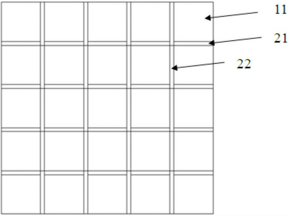
[0043] Provide a crucible, select a square seed crystal with a growth plane orientation of (100) and a side crystal orientation of (110) as the target seed crystal 11, press 5 Lay flat on the bottom of the crucible in a manner of ×5, leave a gap between adjacent target seed crystals, and fill a piece of anisotropic seed crystal 21 with a thickness of 20mm and a cross-sectional size of 156mm*10mm or a cross-sectional size of 176mm*10mm in the gap Anisotropic seed crystal 22, the crystal orientation of the growth plane of the anisotropic seed crystal is (310), and the crystal orientation of the side surface is (100). The close contact between the target seed crystal and the anisotropic seed crystal covers the bottom of the crucible to obtain a seed crystal layer. The thickness of the seed layer is 2cm;

[0044] figure 1 It is a diagram of ...

Embodiment 2

[0046] A method for preparing a quasi-single crystal silicon wafer, comprising the following steps:

[0047] (1) Provide a crucible, select a square seed crystal with a growth plane crystal orientation of (100) and a side crystal orientation of (110) as the target seed crystal, and place 25 target seed crystals with a cross-sectional size of 156mm*156mm and a thickness of 20mm 11 Lay it on the bottom of the crucible in a 5×5 pattern, leave a gap between adjacent target seed crystals, and fill the gap with an anisotropic seed crystal 21 with a thickness of 20mm and a cross-sectional size of 156mm*10mm or a cross-sectional size of 176mm *10mm anisotropic seed crystal 22, the growth surface of the anisotropic seed crystal is (310), the side crystal orientation is (100), the target seed crystal and the anisotropic seed crystal are in close contact with the bottom of the crucible, and the seed crystal is obtained layer, the thickness of the seed layer is 2cm, and the side crystal d...

Embodiment 3

[0058] A method for preparing a quasi-single crystal silicon wafer, comprising the following steps:

[0059] (1) Provide a crucible, select a square seed crystal with a growth plane crystal orientation of (100) and a side crystal orientation of (210) as the target seed crystal, and press 25 target crystal crystals with a cross-sectional size of 156mm*156mm and a thickness of 20mm Spread on the bottom of the crucible in a 5×5 manner, leaving a gap between adjacent target seed crystals, filling the gap with an anisotropic seed crystal with a thickness of 20mm and a cross-sectional size of 156mm*10mm or a cross-sectional size of 176mm*10mm The anisotropic seed crystal, the crystal orientation of the growth plane of the anisotropic seed crystal is (221), and the crystal orientation of the side surface is (110), and the close contact between the target seed crystal and the anisotropic seed crystal covers the bottom of the crucible to obtain a seed crystal layer; The thickness of th...


PUM


Abstract

The invention provides a paving method of seed crystals for casting a pseudo-single crystal silicon wafer. The paving method comprises the following steps: providing a crucible; paving target seed crystals at the bottom of the crucible; reserving a gap between two adjacent target seed crystals and filling the gap with an anisotropic seed crystal, wherein the target seed crystals and the anisotropic seed crystals are tightly contacted and fill the bottom of the crucible to obtain a seed crystal layer; the anisotropic seed crystal comprises a first side face and a second side face which are respectively contacted with the side faces of the two adjacent target seed crystals, the types of crystal boundaries respectively formed by the first and second side faces and the side faces contacted with the adjacent target seed crystals are consistent, and the growth faces of the anisotropic seed crystals is high index crystal faces relative to the growth faces of the target seed crystals. By filling the anisotropic seed crystals in the gaps between two adjacent target seed crystals, dislocation and proliferation of dislocation preferably occur in the anisotropic seed crystals, so that the probability of generating dislocation of the target seed crystals is reduced, and the problem that the pseudo-single crystal prepared in the prior art is more in dislocation is solved.

Description

technical field [0001] The invention relates to the field of semiconductor manufacturing, in particular to a method for laying a seed crystal, a quasi-single crystal silicon wafer and a preparation method thereof. Background technique [0002] At present, the casting methods of quasi-single crystal mainly include seedless crystal seeding and seed crystal seeding method. The seed crystal seeding method is to lay the single crystal seed crystal on the bottom of the quartz crucible first, and keep the seed crystal incompletely melted during the melting stage. , the seeding growth is carried out on the single crystal seed crystal to obtain the quasi-single crystal silicon ingot. When laying the seed crystal, the growth crystal direction of the nucleation surface of the seed crystal is generally guaranteed to be consistent, but the crystal orientation of the side contact surface of the adjacent seed crystal It is usually random, and it is easy to form small-angle grain boundaries...

Claims


Application Information

Patent Timeline
IPC IPC(8): C30B11/14C30B11/00C30B29/06
Inventor 雷琦胡动力何亮陈红荣
Owner JIANGXI SAI WEI LDK SOLAR HI TECH CO LTD
Why Eureka
Try Eureka