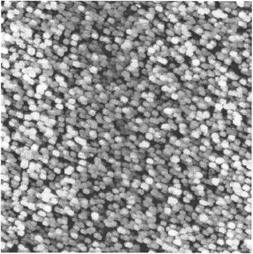
Method for forming buffer layers needed by single-crystal gallium nitride growth
A buffer layer, gallium nitride technology, applied in electrical components, circuits, semiconductor devices, etc., can solve problems such as difficulties, growth film breakage, cracking, etc., to achieve the effect of reducing production time and cost
- Summary
- Abstract
- Description
- Claims
- Application Information
AI Technical Summary
Problems solved by technology
Method used
Image
Examples
Embodiment 1
[0025] A method for forming a buffer layer required for the growth of single crystal gallium nitride, comprising the following steps:
[0026] Step 1): growing a GaN single crystal film on the sapphire substrate according to the HVPE method: including the stage of growing the first buffer layer, the stage of the second buffer layer, and the stage of the third buffer layer;
[0027] Step 2): After the sapphire substrate obtained in step 1) is treated with HCI (treatment temperature is 1100°C), the GaN single crystal film forms a GaN film buffer layer with a nanoporous structure, and the GaN film buffer layer with a nanoporous structure Then grow the first buffer layer, the second buffer layer, and the third buffer layer in sequence, and grow vertical GaN crystals to obtain a GaN single crystal substrate.
[0028] The first buffer layer, the second buffer layer and the third buffer layer are grown with the tendency of V / III ratio gradually decreasing, and the thickness of each l...
Embodiment 2
[0032] A method for forming a buffer layer required for the growth of single crystal gallium nitride, comprising the following steps:
[0033] Step 1): growing a GaN single crystal film on the sapphire substrate according to the HVPE method: including the stage of growing the first buffer layer, the stage of the second buffer layer, and the stage of the third buffer layer;
[0034] Step 2): After the sapphire substrate prepared in step 1) is treated with HCI (treatment temperature is 1000° C.), the GaN single crystal film forms a GaN thin film buffer layer with a nanoporous structure, and the GaN thin film buffer layer with a nanoporous structure Then grow the first buffer layer, the second buffer layer, and the third buffer layer in sequence, and grow vertical GaN crystals to obtain a GaN single crystal substrate.
[0035] The first buffer layer, the second buffer layer and the third buffer layer are grown in the tendency of V / III ratio gradually decreasing, and the thickness...
Embodiment 3
[0037] A method for forming a buffer layer required for the growth of single crystal gallium nitride, comprising the following steps:
[0038] Step 1): growing a GaN single crystal film on the sapphire substrate according to the HVPE method: including the stage of growing the first buffer layer, the stage of the second buffer layer, and the stage of the third buffer layer;
[0039]Step 2): After the sapphire substrate obtained in step 1) is treated with HCI (treatment temperature is 800°C), the GaN single crystal film forms a GaN film buffer layer with a nanoporous structure, and the GaN film buffer layer with a nanoporous structure Then grow the first buffer layer, the second buffer layer, and the third buffer layer in sequence, and grow vertical GaN crystals to obtain a GaN single crystal substrate.
[0040] The first buffer layer, the second buffer layer and the third buffer layer are grown with the V / III ratio gradually decreasing, and the thickness of each layer is 1 μm, ...
PUM
| Property | Measurement | Unit |
|---|---|---|
| thickness | aaaaa | aaaaa |
| thickness | aaaaa | aaaaa |
| thickness | aaaaa | aaaaa |
Abstract
Description
Claims
Application Information
 - R&D Engineer
- R&D Manager
- IP Professional
- Industry Leading Data Capabilities
- Powerful AI technology
- Patent DNA Extraction
Browse by: Latest US Patents, China's latest patents, Technical Efficacy Thesaurus, Application Domain, Technology Topic.
© 2024 PatSnap. All rights reserved.Legal|Privacy policy|Modern Slavery Act Transparency Statement|Sitemap

