Surrounding-gate field effect transistor and fabrication method thereof

A field-effect transistor and gate-around technology, which is applied in the field of gate-around field effect transistors and its preparation, can solve problems such as the complexity of GAA source and drain design, and achieve the effects of solving thermal stability problems, good gate control ability, and suppressing short channel effects

Active Publication Date: 2014-11-19
PEKING UNIV
View PDF5 Cites 10 Cited by
  • Summary
  • Abstract
  • Description
  • Claims
  • Application Information

AI Technical Summary

Problems solved by technology

In addition, the introduction of nanowires makes the source and drain

Method used


Image

  • Surrounding-gate field effect transistor and fabrication method thereof
  • Surrounding-gate field effect transistor and fabrication method thereof
  • Surrounding-gate field effect transistor and fabrication method thereof

Examples


Embodiment Construction

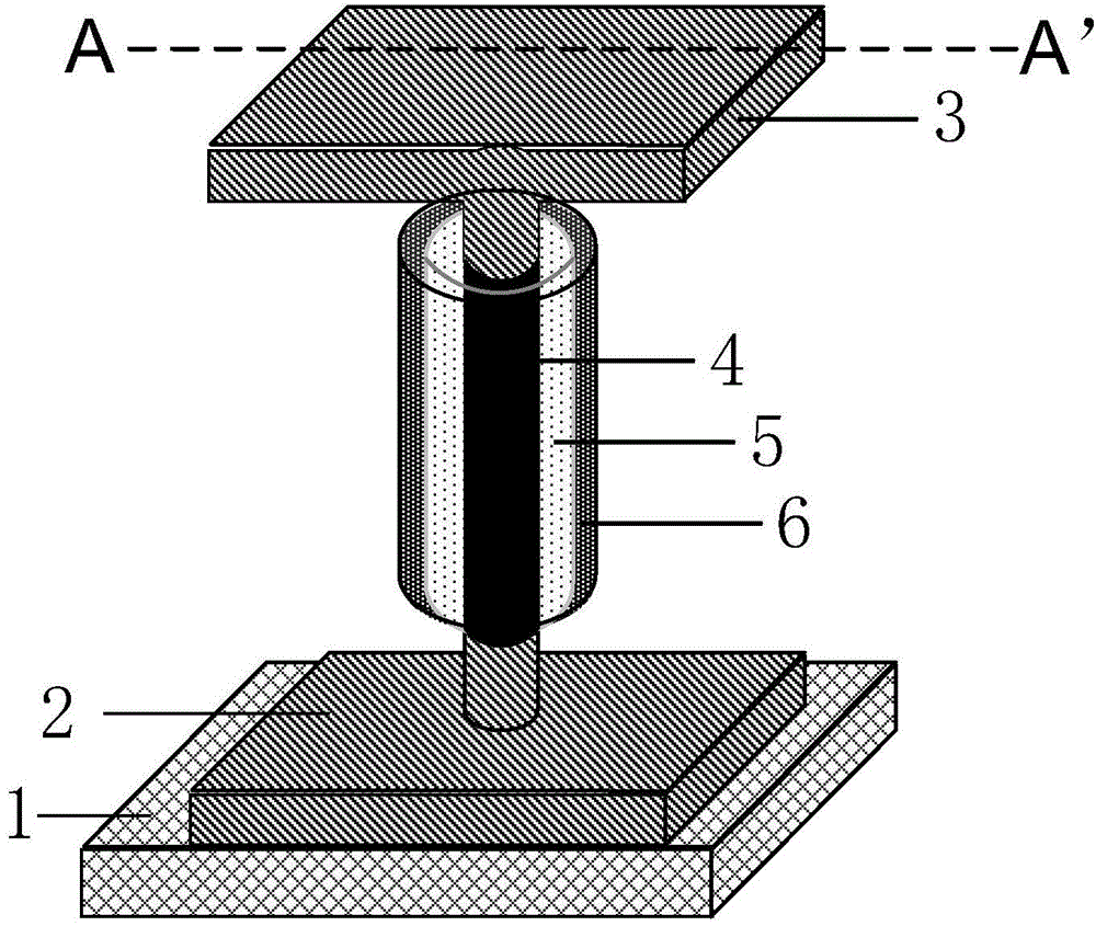
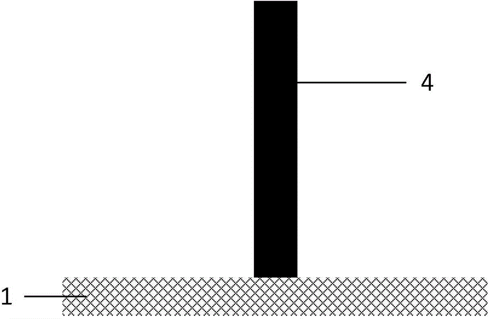
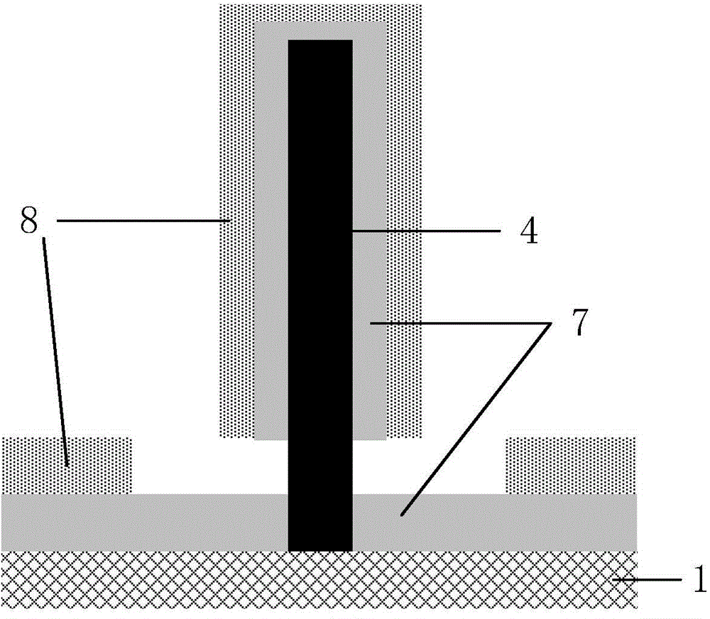
[0041] The present invention provides a field effect transistor with a novel structure, specifically a gate-around field effect transistor combined with a vertical channel and a Schottky barrier source / drain structure (such as figure 1 shown), including a ring-shaped semiconductor channel 4 in a vertical direction, a ring-shaped gate electrode 6, a ring-shaped gate dielectric layer 5, a source region 2, a drain region 3, and a semiconductor substrate 1; wherein, the source The region 2 is located at the bottom of the vertical channel 4 and is in contact with the substrate 1. The drain region 3 is located at the top of the vertical channel 4. The gate dielectric layer 5 and the gate electrode 6 surround the vertical channel 4 in a ring shape; the source region 2 and the The drain regions 3 form Schottky contacts with the channels 4 respectively.

[0042] The source region and the drain region can be any metal with good conductivity or a compound formed of metal and substrate ma...


PUM


Abstract

The invention discloses a surrounding-gate field effect transistor, which combines a vertical channel and a Schottky barrier source/drain structure. The surrounding-gate field effect transistor comprises a surrounding semiconductor channel (4) in the vertical direction, a surrounding gate electrode (6), a surrounding gate dielectric layer (5), a source region (2), a drain region (3) and a semiconductor substrate (1), wherein the source region (2) is located at the bottom part of the vertical channel (4) and is connected with the substrate (1); the drain region (3) is located at the top part of the vertical channel (4); the gate dielectric layer (5) and the gate electrode (6) surround the vertical channel (4); Schottky contact with the same barrier height is respectively formed between the source region (2) and the drain region (3) and the channel (4); and the source region and the drain region use the same metal material. The structure uses the Schottky barrier source/drain structure so as to reduce thermal budget, reduce serial resistance and parasitic capacitance and simplify technology requirements, and uses the vertical channel and the surrounding gate structure so as to break through limitation of integrated processing lithography limit and improve the degree of integration.

Description

technical field [0001] The invention belongs to the field of field effect transistor logic devices and circuits in CMOS ultra-large integrated circuits (ULSI), and in particular relates to a ring gate field effect transistor combined with a vertical channel and a Schottky barrier source / drain structure and a preparation method thereof. Background technique [0002] Driven by Moore's Law, the feature size of traditional MOSFETs has been shrinking, and now it has entered the nanometer scale. As a result, the negative effects of short-channel effects on devices have become more serious. The effects of leakage-induced barrier reduction and band-band tunneling increase the off-state leakage current of the device. In the research on new device structures, the source-drain doped Gate All Around transistor (GAA) structure is currently the most concerned one. GAA devices have better gate control characteristics, which can meet the sharpest characteristic requirements, so as to meet ...

Claims


Application Information

Patent Timeline
IPC IPC(8): H01L29/78H01L29/423H01L21/336
CPCH01L29/1037H01L29/4236H01L29/66666H01L29/7827H01L29/7839
Inventor 孙雷徐浩张一博韩静文王漪张盛东
Owner PEKING UNIV
Why Eureka
Try Eureka