Method for forming electroconductive pattern, and electroconductive pattern substrate

A conductive pattern and substrate technology, which can be applied to equipment for manufacturing conductive/semiconductive layers, components of conductive cores, lithography/patterns, etc. Large burden and other problems, to achieve the effect of sufficient adhesion

Active Publication Date: 2014-11-26
HITACHI CHEM CO LTD
View PDF7 Cites 6 Cited by
  • Summary
  • Abstract
  • Description
  • Claims
  • Application Information

AI Technical Summary

Problems solved by technology

[0005] ITO films, tin oxide films, etc. are usually formed by sputtering, but the properties of transparent conductive films are likely to change depending on the sputtering method, sputtering power, air pressure, substrate temperature, and the type of atmospheric gas.
The difference in the film quality of the transparent conductive film caused by the change of the sputtering condition becomes the cause of the variation in the etching rate when the transparent conductive film is wet-etched, and the yield of the product is likely to decrease due to poor pattern formation
In addition, the above-mentioned method of forming a conductive pattern includes a sputtering process, a resist forming process, and an etching process, and the process is long, which imposes a large cost burden.

Method used


Image

  • Method for forming electroconductive pattern, and electroconductive pattern substrate
  • Method for forming electroconductive pattern, and electroconductive pattern substrate
  • Method for forming electroconductive pattern, and electroconductive pattern substrate

Examples


Embodiment 1

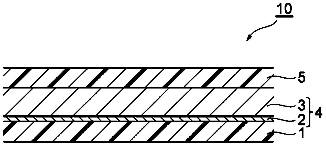
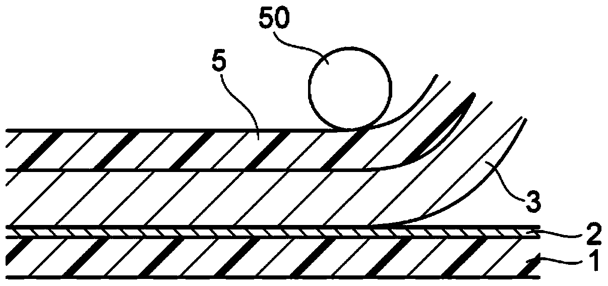
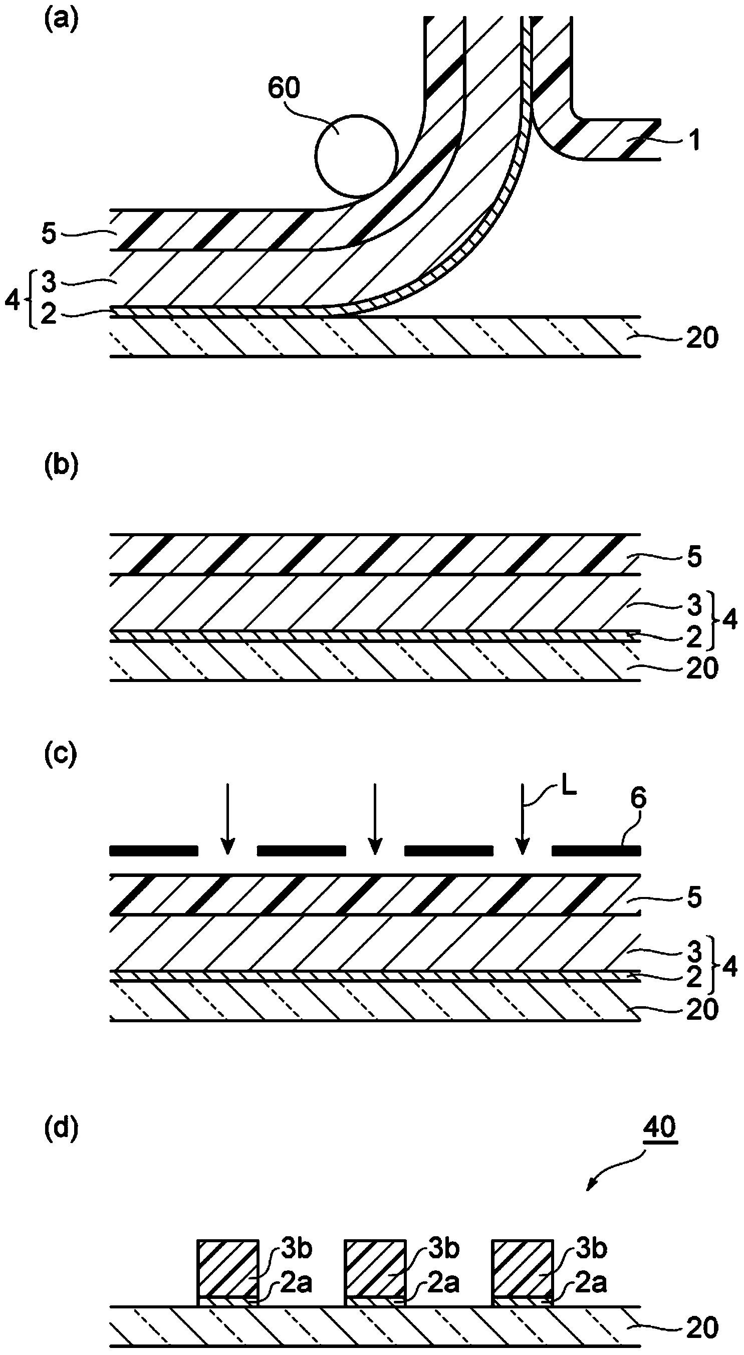
[0150] On a polyethylene terephthalate film (PET film, manufactured by Teijin Co., Ltd., trade name: G2-16) with a thickness of 16 μm as a support film, the 2 Uniformly apply the above-mentioned conductive fiber dispersion liquid 1, dry it with a hot air convection dryer at 100°C for 10 minutes, and pressurize it with a linear pressure of 1 MPa at room temperature (25°C), thereby forming a layer containing conductive fibers on the support film. The conductive layer of the fiber. In addition, the film thickness after drying of the conductive layer was about 0.1 micrometer as a result of the measurement by the scanning electron micrograph.

[0151] Next, the solution of the above-mentioned photosensitive resin composition was evenly coated on a polyethylene terephthalate film (PET film, manufactured by Teijin Co., Ltd., trade name: G2-50) with a thickness of 50 μm prepared separately, It dried for 10 minutes with the hot-air convection type dryer of 100 degreeC, and formed the ...


PUM

PropertyMeasurementUnit
diameteraaaaaaaaaa
thicknessaaaaaaaaaa
diameteraaaaaaaaaa

Abstract

This method for forming an electroconductive pattern is provided with: a lamination step for readying a photosensitive electroconductive film provided with a support film, an electroconductive layer including electroconductive fiber, and a photosensitive resin layer including a photosensitive resin, in the sequence listed, and laminating the electroconductive layer and the photosensitive resin layer so that the electroconductive layer is on a base material in intimate contact; and a patterning step for exposing and developing the photosensitive resin layer on the base material and thereby forming an electroconductive pattern.

Description

technical field [0001] The present invention relates to a method for forming a conductive pattern and a substrate with a conductive pattern, especially a method for forming a conductive pattern and a conductive pattern used as electrode wiring of flat panel displays such as liquid crystal display elements, touch panels (touch panels), solar cells, and lighting. substrate. Background technique [0002] Devices using liquid crystal display elements, touch panels, etc. are becoming popular in large electronic devices such as personal computers and televisions, small electronic devices such as car navigation systems, mobile phones, and electronic dictionaries, and display devices such as OA and FA devices. In these liquid crystal display elements and touch panels, a transparent conductive film is used for wiring, pixel electrodes, or a part of terminals that are required to be transparent. In addition, transparent conductive films are also used in devices such as solar cells an...

Claims


Application Information

Patent Timeline
Patent Type & Authority Applications(China)
IPC IPC(8): H01B13/00H01B5/14H05K3/02
CPCH05K1/092H01L31/1884H05K2203/0514H05K3/02H05K2201/0281H01B5/14H01B5/16H01B7/0027H01B13/00H01B13/0026Y02E10/50
Inventor 田仲裕之山崎宏五十岚由三伊藤豊树太田绘美子
Owner HITACHI CHEM CO LTD
Why Eureka
Try Eureka