Method for manufacturing selective tensile stress contact hole etching stop layers

A technology of contact hole etching and manufacturing method, which is applied in semiconductor/solid-state device manufacturing, electrical components, circuits, etc., can solve problems such as adverse effects on the electrical performance of PMOS devices, and achieve the effects of low cost, avoiding complexity, and simple process

Inactive Publication Date: 2014-12-03
SHANGHAI HUALI MICROELECTRONICS CORP
View PDF3 Cites 5 Cited by
  • Summary
  • Abstract
  • Description
  • Claims
  • Application Information

AI Technical Summary

Problems solved by technology

[0006] However, the Single CESL process is used to simultaneously form a high tensile stress silicon nitride contact hole etch stop layer with ultimate stress in the PMOS region and NMOS region after UV curing, and the existence of the high tensile stress silicon nitride with ultimate stress has a negative effect on The electrical performance of PMOS devices is adversely affected, so the Single CESL process is a compromise method at the expense of hole mobility in PMOS devices.

Method used


Image

  • Method for manufacturing selective tensile stress contact hole etching stop layers
  • Method for manufacturing selective tensile stress contact hole etching stop layers
  • Method for manufacturing selective tensile stress contact hole etching stop layers

Examples


Embodiment Construction

[0032] The specific embodiment of the present invention will be further described in detail below in conjunction with the accompanying drawings. Of course, the present invention is not limited to the following specific embodiments, and general replacements known to those skilled in the art are also covered within the protection scope of the present invention.

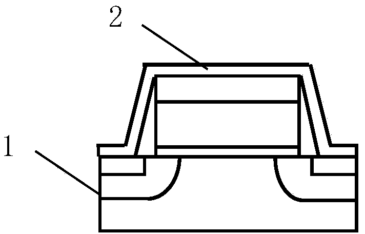
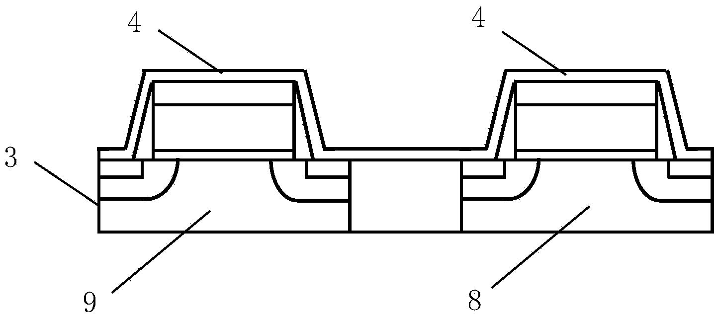
[0033] It should be noted that, in the following examples, using Figure 3 ~ Figure 11 The schematic diagram in the figure describes in detail the device structure formed according to the method for manufacturing the etching stop layer of the double contact hole of the present invention. When describing the embodiments of the present invention in detail, for the convenience of illustration, the schematic diagrams are not drawn according to the general scale and partially enlarged and omitted. Therefore, it should be avoided as a limitation of the present invention.

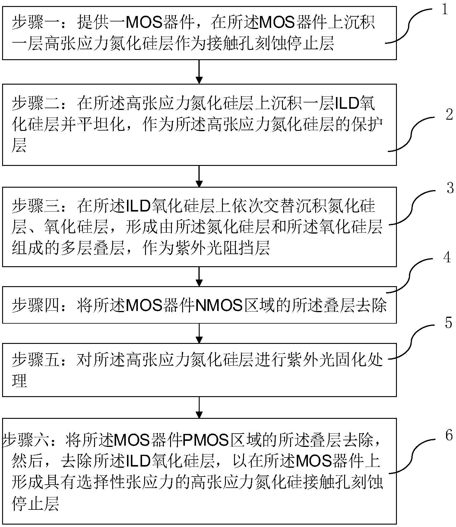
[0034] see figure 2 , figure 2 It is a flow char...


PUM

PropertyMeasurementUnit
refractive indexaaaaaaaaaa

Abstract

The invention discloses a method for manufacturing selective tensile stress contact hole etching stop layers. The method comprises the steps that a high tensile stress silicon nitride layer is deposed on an MOS device to be used as a contact hole etching stop layer, a multiple-laminating layer composed of a silicon nitride layer and a silicon oxide layer in an alternative mode is used as a ultraviolet light blocking layer of a PMOS area, the high tensile stress silicon nitride layer on the PMOS area and an NMOS area is subjected to selective ultraviolet light polymerization processing, a high tensile stress silicon nitride layer with the relative low stress covers the PMOS area, a high tensile stress silicon nitride layer with the relative high stress covers the NMOS area, and the purpose that the PMOS area and the NMOS area are provided with selective silicon nitride contact hole etching stop layers with different high tensile stress is achieved, the negative influence on the hole mobility of a PMOS device of single-step high tensile stress silicon nitride deposition is avoided, the complexity of a process for forming two contact hole etching stop layers by two-step silicon nitride deposition is also avoided, and the electrical property of the device is improved by low cost.

Description

technical field [0001] The invention relates to the technical field of semiconductor integrated circuit manufacturing, and more specifically, to a method for manufacturing a selective tensile stress contact hole etching stop layer based on strained silicon technology and improving device performance through high-stress silicon nitride. Background technique [0002] With the development of CMOS integrated circuit manufacturing process and the reduction of critical dimensions, many new methods are applied to device manufacturing process to improve device performance. Among them, the high-stress silicon nitride film is introduced into the integrated circuit manufacturing process because it can effectively improve the carrier mobility of the MOS tube, thereby increasing the operating speed of the device. The compressive stress in the direction of the PMOS channel can improve the hole mobility in the PMOS device, and the tensile stress in the direction of the NMOS channel can imp...

Claims


Application Information

Patent Timeline
Patent Type & Authority Applications(China)
IPC IPC(8): H01L21/8238H01L21/318H01L21/316H01L21/3105
CPCH01L21/8238H01L21/3105H01L21/823871
Inventor 雷通
Owner SHANGHAI HUALI MICROELECTRONICS CORP
Why Eureka
Try Eureka