Low temperature solid state bonding method through surface micro-nano structure

A micro-nano structure and bonding technology, used in semiconductor/solid-state device manufacturing, electrical solid-state devices, electrical components, etc., can solve the problems of low welding strength and high welding temperature, and achieve good bonding performance, high conductivity, and good plasticity. deformable effect

Inactive Publication Date: 2014-12-10
SHANGHAI JIAO TONG UNIV
View PDF4 Cites 15 Cited by
  • Summary
  • Abstract
  • Description
  • Claims
  • Application Information

AI Technical Summary

Problems solved by technology

[0004] In view of the problems existing in the above-mentioned prior art, the present invention proposes a low-temperature solid-state bonding method using surface micro-nano structures, which overcomes the problems of high soldering temperature and low soldering strength in the existing packaging and interconnection process

Method used


Image

  • Low temperature solid state bonding method through surface micro-nano structure
  • Low temperature solid state bonding method through surface micro-nano structure
  • Low temperature solid state bonding method through surface micro-nano structure

Examples


Embodiment Construction

[0024] The embodiments of the present invention are described in detail below. This embodiment is implemented on the premise of the technical solution of the present invention, and detailed implementation methods and specific operating procedures are provided, but the protection scope of the present invention is not limited to the following implementation example.

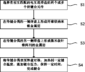
[0025] The invention provides a low-temperature solid-state bonding method utilizing surface micro-nano structures, comprising the following steps:

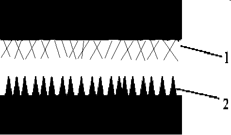
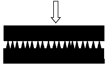
[0026] S1: Select two chips or substrates with matching electrical interconnection pads;

[0027] S2: Preparation of fibrous nano-silver metal layer: After degreasing the surface of the metal block in the bonding area of ​​the chip or substrate, immerse it in 20wt.% sulfuric acid to activate it to improve the surface activity, and then place it in the chemical deposition solution for chemical deposition , thus obtaining the desired fibrous nano-silver metal layer 1; ...


PUM

PropertyMeasurementUnit
lengthaaaaaaaaaa
thicknessaaaaaaaaaa
diameteraaaaaaaaaa

Abstract

The invention discloses a low temperature solid state bonding method through a surface micro-nano structure. The low temperature solid state bonding method through the surface micro-nano structure comprises choosing two or more elements to be bonded with matching electrical interconnecting pads, wherein every two elements forms a to-be-boned couple; forming fiber-shaped nano silver metal layers on pads on one side of the to-be-boned couples; forming a metal layer of a micron size cone array structure on the pads of the other sides of the to-be-boned couples; aligning pads on the surfaces of the to-be-boned couples, and heating contact areas to a certain temperature lower than a metal melting point and meanwhile applying pressure to one or two sides of the to-be-boned couples and maintaining the state for a certain period to enable the fiber-shaped nano silver metal layers to be in solid state bonding with the metal layers of the micron size cone array structure. According to the low temperature solid state bonding method through the surface micro-nano structure, the conductivity and the electrical conductivity are higher, temperature of thermocompression bonding can be greatly reduced and bonding strength is improved.

Description

technical field [0001] The invention relates to the field of semiconductor chip packaging, in particular to a method for realizing low-temperature interconnection and bonding through the use of a fibrous nano-silver metal layer and a metal layer with a special needle cone shape on the surface. Background technique [0002] At present, electronic packaging is developing towards miniaturization, high density and multi-chip, and electrical interconnection technology is the core technology in electronic packaging technology. According to Moore's Law, the power of package components continues to rise and the pin density continues to increase, making them need to serve at higher and higher temperatures to ensure long-term reliability. However, the traditional reflow soldering process needs to heat the temperature above the melting point of the solder. The high temperature environment will have a bad impact on the chip itself, greatly reducing the reliability of the product, and ac...

Claims


Application Information

Patent Timeline
Patent Type & Authority Applications(China)
IPC IPC(8): H01L21/603
CPCH01L24/83H01L2224/84H01L2224/84203
Inventor 胡丰田李明胡安民吴蕴雯
Owner SHANGHAI JIAO TONG UNIV
Why Eureka
Try Eureka