Production method of infrared light-emitting diode with high-reliability electrodes

A technology of infrared luminescence and manufacturing method, which is applied in the direction of circuits, electrical components, semiconductor devices, etc., can solve the problems of easily broken soldering station electrodes and the peeling off of the epitaxial layer of soldering station electrodes, so as to increase the contact surface, increase the current expansion, and improve The effect of luminous efficiency

Inactive Publication Date: 2014-12-10
XIAMEN CHANGELIGHT CO LTD
View PDF4 Cites 4 Cited by
  • Summary
  • Abstract
  • Description
  • Claims
  • Application Information

AI Technical Summary

Problems solved by technology

[0005] The purpose of the present invention is to provide a method for manufacturing infrared light-emitting diodes with high-reliability electrodes, which can effectively improve the reliability of the electrodes, and solve the

Method used


Image

  • Production method of infrared light-emitting diode with high-reliability electrodes
  • Production method of infrared light-emitting diode with high-reliability electrodes
  • Production method of infrared light-emitting diode with high-reliability electrodes

Examples


Embodiment 1

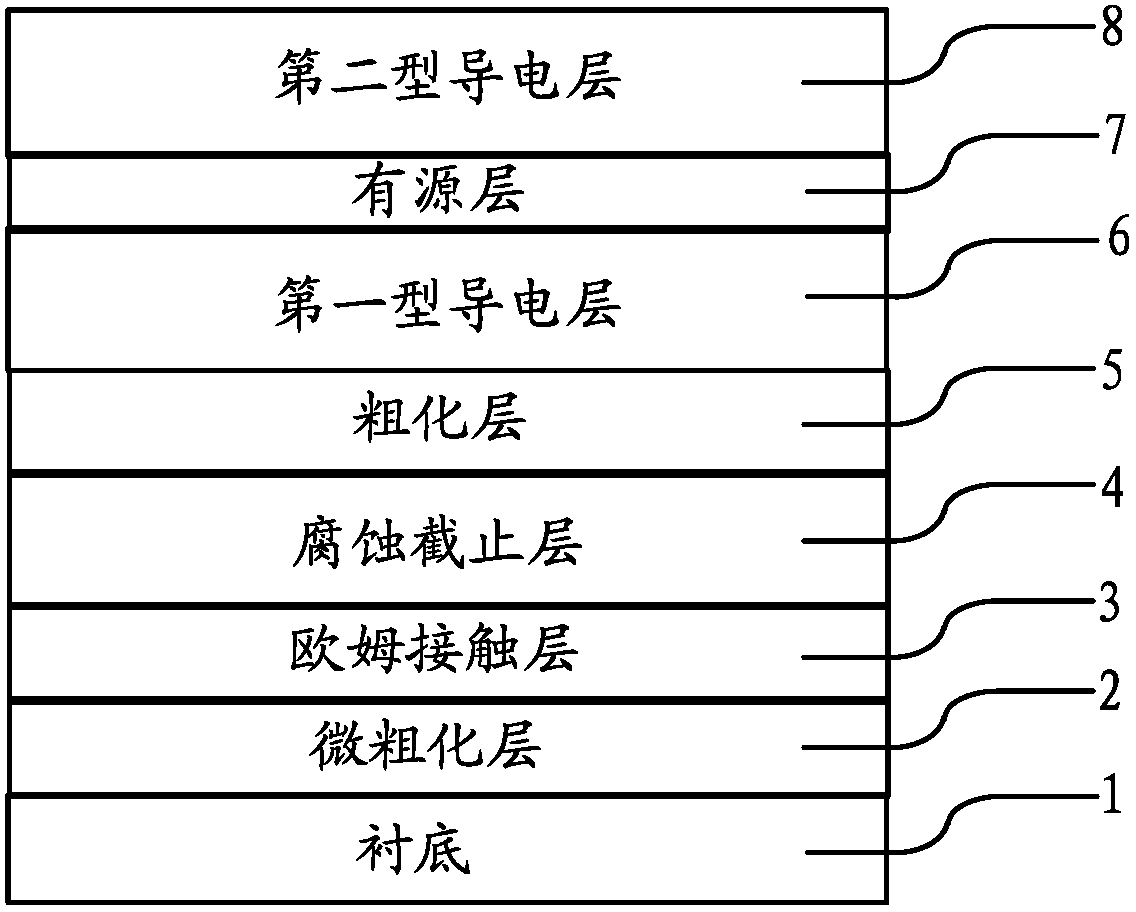
[0049] refer to Figure 1 to Figure 7 As shown, the present invention discloses an infrared light-emitting diode with high-reliability electrodes and the first embodiment of its manufacturing method.

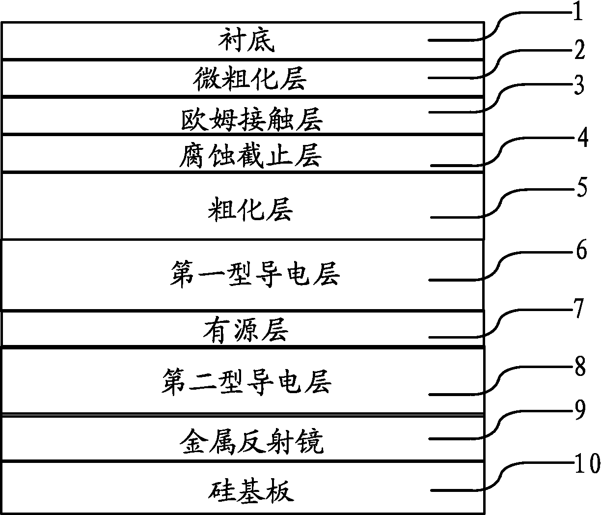
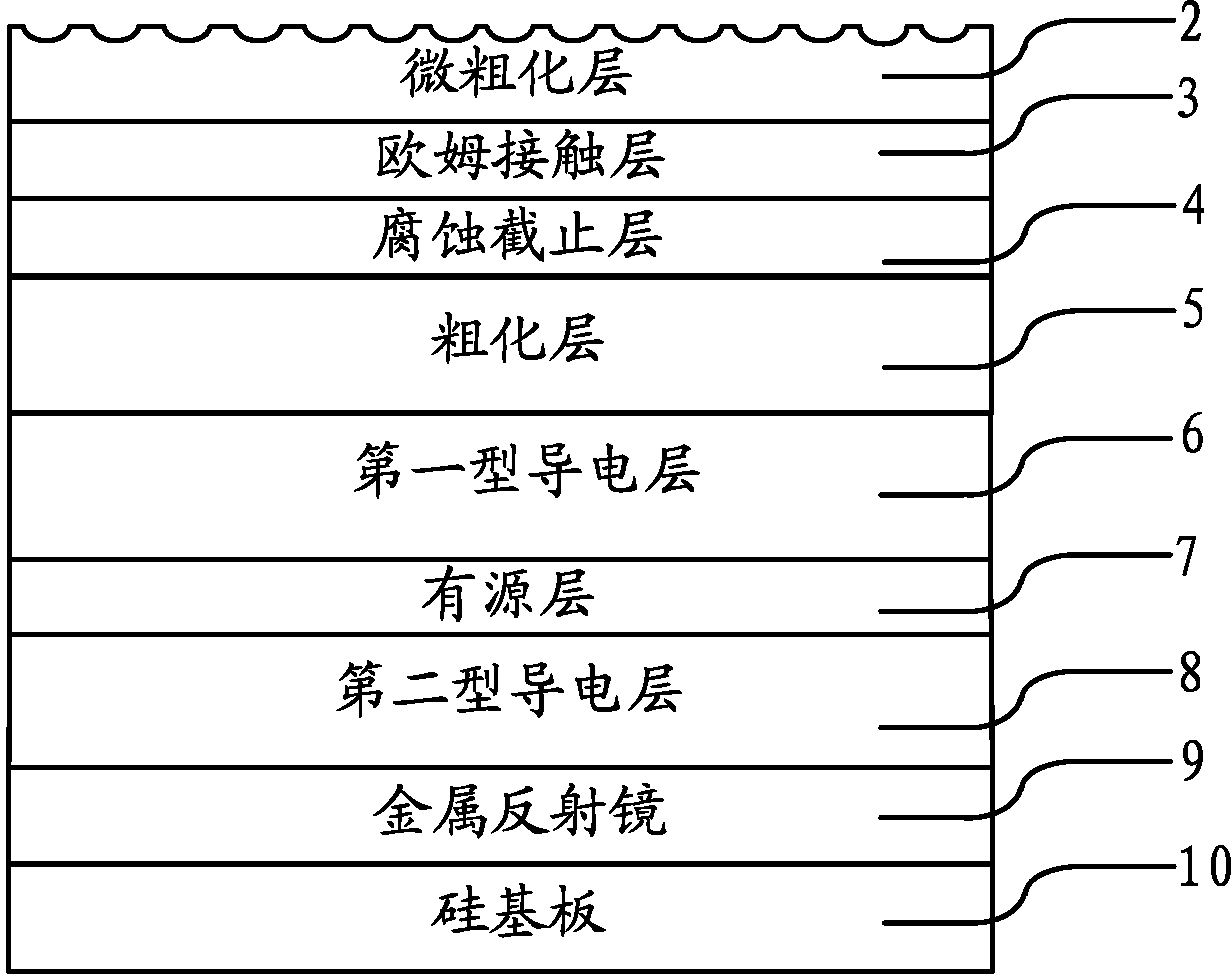
[0050] Such as figure 1 As shown, the upper surface of the GaAs substrate 1 is composed of a micro-roughened layer 2, an ohmic contact layer 3, an etching stop layer 4, a roughened layer 5, a first-type conductive layer 6, an active layer 7, and a first-type conductive layer 6 from bottom to top. Type II conductive layer 8 .

[0051] The material of the micro-roughened layer 2 is (Al 0.5 Ga 0.5 ) 0.5 In 0.5 P three and five compounds, and the thickness of the micro-roughened layer is 200nm.

[0052] The material of the ohmic contact layer 3 is GaAs III-V compound, and the thickness of the ohmic contact layer 3 is 100 nm.

[0053] The material of corrosion stop layer 4 comprises (Al 0.5 Ga 0.5 ) 0.5 In 0.5 P three and five compounds, and the thickness of the corrosion st...

Embodiment 2

[0069] The difference between embodiment two and embodiment one is: the material of the micro-roughened layer 2 is (Al 0.4 Ga 0.6 ) 0.5 In 0.5 P three and five compound, and the thickness of the micro-roughened layer 2 is 300nm.

[0070] The material of the ohmic contact layer 3 is GaAs III-V compound, and the thickness of the ohmic contact layer 3 is 150 nm.

[0071] The material of the corrosion stop layer 4 includes (Al 0.8 Ga 0.2 ) 0.5 In 0.5 P three and five compounds, and the thickness of the corrosion stop layer 4 is 150nm.

[0072] The material of the roughened layer 5 is Al 0.45 Ga 0.55 As III-V compound, and the thickness of the roughened layer 5 is 2 μm.


PUM

PropertyMeasurementUnit
Surface roughnessaaaaaaaaaa
Thicknessaaaaaaaaaa
Thicknessaaaaaaaaaa

Abstract

The invention discloses a production method of an infrared light-emitting diode with high-reliability electrodes. The production method includes: providing an epitaxial layer, evaporating a metal reflector on a second-type conducting layer of the epitaxial layer, and bonding the metal reflector on the substrate; removing the epitaxial substrate, and exposing a micro roughening layer; forming roughening morphology on the surface of the micro roughening layer; removing part of the micro roughening layer, producing a bonding pad electrode in the rest area of the micro roughening layer, and exposing an ohmic contact layer in the removed area of the micro roughening layer; forming extension electrode patterns on the surface of the exposed ohmic contact layer; forming the bonding pad electrode and extension electrodes; removing the exposed ohmic contact layer and an corrosion stop layer in a layer-by-layer manner till a roughening layer is exposed; forming surface roughening morphology in the exposed area of the roughening area; evaporating a back electrode on the back of the substrate, and performing fragmentation. By the method, reliability of soldering station electrodes is improved effectively, the problem that soldering station electrodes are prone to falling off due to poor adhesion is solved, and the packaging problem that the epitaxial layer under the soldering station electrodes is easy to break up during wire bonding is solved as well.

Description

technical field [0001] The invention relates to the technical field of light-emitting diodes, in particular to a method for manufacturing an infrared light-emitting diode with high-reliability electrodes. Background technique [0002] Infrared light-emitting diodes have the advantages of low power consumption, small size and high reliability, and are widely used in communication, remote sensing devices and other fields. In the prior art, metal-organic compound vapor phase epitaxy is used to grow the epitaxial structure with quantum wells to achieve higher internal quantum efficiency; at the same time, flip-chip manufacturing processes such as metal mirrors and surface roughening are used to improve the external quantum efficiency of infrared light-emitting diodes. efficiency. [0003] Due to the complicated steps of the flip-chip process, the reliability of electrodes produced by the manufacturing process adopted in the prior art is relatively poor. The publication number ...

Claims


Application Information

Patent Timeline
IPC IPC(8): H01L33/30H01L33/40H01L33/38
CPCH01L33/10H01L33/007H01L33/22H01L33/32
Inventor 林志伟陈凯轩张永杨凯蔡建九白继锋卓祥景姜伟刘碧霞
Owner XIAMEN CHANGELIGHT CO LTD
Why Eureka
Try Eureka