Organic light emission diode device and preparation method thereof

An electroluminescent device and luminescent technology, which is applied in the direction of electric solid-state devices, semiconductor/solid-state device manufacturing, electrical components, etc., can solve the problems of low device life and low luminous efficiency of organic electroluminescent devices, and achieve film-forming quality Good, beneficial to the transmission process and the effect of increasing the number

Inactive Publication Date: 2014-12-17
OCEANS KING LIGHTING SCI&TECH CO LTD +2
View PDF3 Cites 1 Cited by
  • Summary
  • Abstract
  • Description
  • Claims
  • Application Information

AI Technical Summary

Problems solved by technology

[0003] So far, although researchers from all over the world have greatly improved the performance indicators of the device by selecting suitable organic materials and reasonable device structure design, due to the large current driving the light-emitting device, As a result, orga

Method used


Image

  • Organic light emission diode device and preparation method thereof
  • Organic light emission diode device and preparation method thereof

Examples


Embodiment 1

[0028] A method for preparing an organic electroluminescent device, comprising the following steps:

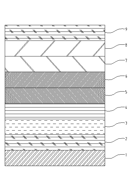
[0029] (1) A glass substrate is provided, and a conductive anode is deposited on the surface of the glass substrate by electron beam evaporation, and the conductive anode is Ag, among which,

[0030] The pressure when preparing the conductive anode by electron beam evaporation is 1×10 -3 Pa, the energy density of electron beam evaporation is 10W / cm2 , the evaporation rate is 0.01 nm / s, and the thickness of the conductive anode is 20nm.

[0031] (2) Vacuum-deposit the first hole injection auxiliary layer on the surface of the conductive anode. The material of the first hole injection auxiliary layer is 2,3,6,7,10,11-hexacyano-1,4,5, 8,9,12-hexaazatriphenylene (HAT-CN), the pressure of the first hole injection auxiliary layer evaporation is 1×10 -3 Pa, the evaporation rate is 0.1nm / s, and the evaporation thickness is 1nm.

[0032] (3) The second hole injection auxiliary ...

Embodiment 2

[0043] A method for preparing an organic electroluminescent device, comprising the following steps:

[0044] (1) A glass substrate is provided, and a conductive anode is deposited on the surface of the substrate through vacuum thermal resistance evaporation, and the conductive anode is selected from Al. Among them,

[0045] The pressure of conductive anode evaporation is 1×10 -5 Pa, the evaporation rate is 5nm / s.

[0046] (2) Vacuum-deposit the first hole injection auxiliary layer on the surface of the conductive anode. The material of the first hole injection auxiliary layer is 2,3,6,7,10,11-hexacyano-1,4,5, 8,9,12-hexaazatriphenylene (HAT-CN), the first hole injection auxiliary layer was evaporated at a pressure of 1×10 -5 Pa, the evaporation rate is 1nm / s, and the evaporation thickness is 5nm.

[0047] (3) The second hole injection auxiliary layer is vacuum evaporated on the surface of the first hole injection auxiliary layer. The material of the second hole injection au...

Embodiment 3

[0058] A method for preparing an organic electroluminescent device, comprising the following steps:

[0059] (1) A glass substrate is provided, and a conductive anode is prepared by electron beam evaporation on the surface of the glass substrate. The conductive anode is selected from Au, wherein,

[0060] The pressure when the conductive anode is evaporated by electron beam is 1×10 -4 Pa, the energy density of electron beam evaporation is 100W / cm 2 , the evaporation rate is 1nm / s, and the thickness of the conductive anode is 100nm.

[0061] (2) Vacuum-deposit the first hole injection auxiliary layer on the surface of the conductive anode. The material of the first hole injection auxiliary layer is 2,3,6,7,10,11-hexacyano-1,4,5, 8,9,12-hexaazatriphenylene (HAT-CN), the first hole injection auxiliary layer was evaporated at a pressure of 1×10 -4 Pa, the evaporation rate is 0.5nm / s, and the evaporation thickness is 2nm.

[0062] (3) The second hole injection auxiliary layer ...


PUM

PropertyMeasurementUnit
Thicknessaaaaaaaaaa
Thicknessaaaaaaaaaa
Thicknessaaaaaaaaaa

Abstract

The invention discloses an organic light emission diode device. The organic light emission diode device comprises a substrate, a conductive anode, a first hole injection auxiliary layer, a second hole injection auxiliary layer, a hole transmission layer, a luminous layer, an electronic transmission layer, an electronic injection layer and a cathode, which are stacked in sequence, wherein the first hole injection auxiliary layer is made of 2,3,6,7,10,11-hexacyano-1,4,5,8,9,12-hexaazatriphenylene, and the second hole injection auxiliary layer is made of zinc phthalocyanine, copper phthalocyanine, oxyvanadium phthalocyanine or titanyl phthalocyanine. The invention also discloses a preparation method of the organic light emission diode device. According to the preparation method of the organic light emission diode device, through adding two layers of hole injection auxiliary layers in the conductive anode and the hole transmission layer for improving the hole injection capacity, the organic light emission diode device prepared by utilizing the preparation method of the organic light emission diode device has the advantages of small drive current and high luminous efficiency.

Description

technical field [0001] The invention relates to the field of organic electroluminescence, in particular to an organic electroluminescence device and a preparation method thereof. Background technique [0002] Organic light-emitting devices (Organic light-emitting DeVices, referred to as OLEDs) is a multi-layer light-emitting device using organic light-emitting materials, including sequentially stacked anode layer, hole injection layer, hole transport layer, light-emitting layer, electron transport layer layer and cathode. The luminescent principle of OLED is based on the action of an external electric field, electrons are injected from the cathode to the lowest unoccupied molecular orbital (LUMO) of organic matter, and holes are injected from the anode to the highest occupied orbital (HOMO) of organic matter. The light-emitting layers meet, recombine, and form excitons. The excitons migrate under the action of the electric field and transfer energy to the light-emitting mat...

Claims


Application Information

Patent Timeline
IPC IPC(8): H01L51/50H01L51/54H01L51/56
CPCH10K85/649H10K85/321H10K85/331H10K85/341H10K85/371H10K85/381H10K50/15H10K50/81H10K71/00
Inventor 周明杰冯小明张振华王平
Owner OCEANS KING LIGHTING SCI&TECH CO LTD
Why Eureka
Try Eureka