Method for manufacturing flexible copper-clad plate with metalized through hole
A flexible copper clad laminate and metallized via technology, which is applied in the manufacture of printed circuits, the formation of electrical connection of printed components, and electrical components, etc., can solve the problems of complex process, long process and high cost, and can simplify the process and improve the electrical conductivity. Effect
- Summary
- Abstract
- Description
- Claims
- Application Information
AI Technical Summary
Problems solved by technology
Method used
Image
Examples
no. 1 example
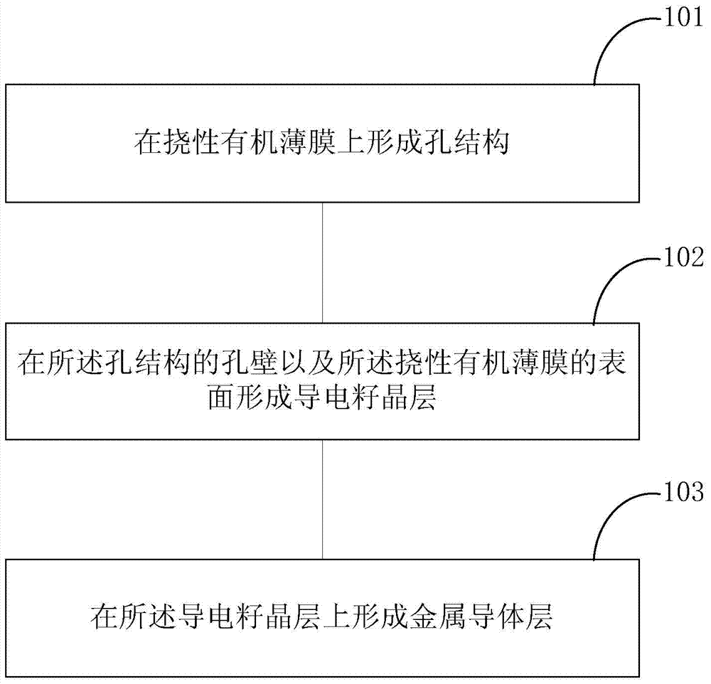
[0032] figure 1 It is an implementation flow chart of the method for manufacturing a flexible copper clad laminate with metalized vias provided by the first embodiment of the present invention. Such as figure 1 As shown, the method provided by the embodiment of the present invention includes:
[0033] Step 101, forming a hole structure on the flexible organic film.
[0034] Figure 2b It is the corresponding structural diagram in this step of the method for manufacturing a flexible copper clad laminate with metalized vias provided by an embodiment of the present invention. Reference Figure 2a with 2b , In such as Figure 2a The flexible organic film 201 shown is formed as Figure 2b The pore structure 211 shown.
[0035] Preferably, the flexible organic film may include: polyimide film, liquid crystal polymer film, polyethylene urea film, polystyrene film, polyethylene terephthalate film, polytetrafluoroethylene Film or polyethylene naphthalate film.
[0036] Preferably, the shape ...
no. 2 example
[0056] image 3 It is an implementation flowchart of a method for manufacturing a flexible copper clad laminate with metalized vias according to the second embodiment of the present invention. Such as image 3 As shown, the method provided by the embodiment of the present invention includes:
[0057] Step 301, forming a hole structure on the flexible organic film.
[0058] Preferably, the flexible organic film may include: polyimide film, liquid crystal polymer film, polyethylene urea film, polystyrene film, polyethylene terephthalate film, polytetrafluoroethylene Film or polyethylene naphthalate film.
[0059] Preferably, the shape of the hole structure is round or square.
[0060] Preferably, the method for forming a hole structure on the flexible organic film is selected from one or more of the following groups: mechanical drilling, punching, laser drilling, and plasma etching.
[0061] Step 302, using a vapor deposition process to form a conductive seed layer on the hole wall of t...
no. 3 example
[0070] Figure 4 It is an implementation flowchart of a method for manufacturing a flexible copper clad laminate with metalized vias provided by the third embodiment of the present invention. Such as Figure 4 As shown, the method provided by the embodiment of the present invention includes:
[0071] Step 401, forming a hole structure on the flexible copper clad board.
[0072] Preferably, the structure for forming holes on the flexible copper clad plate is selected from one or more of the following group: mechanical drilling, punching, laser drilling, plasma etching and reactive ion etching.
[0073] Step 402, using a vapor deposition process to form a conductive seed layer on the hole wall of the hole structure and the surface of the flexible copper clad laminate.
[0074] Compared with the prior art that uses electroless copper plating or black hole processes to form a conductive seed layer, the above solution uses a vapor deposition process to form conductive seeds on the hole wal...
PUM
| Property | Measurement | Unit |
|---|---|---|
| Thickness | aaaaa | aaaaa |
| Sheet resistance | aaaaa | aaaaa |
| Thickness | aaaaa | aaaaa |
Abstract
Description
Claims
Application Information


