Method for forming metal pad and semiconductor structure

A metal pad and metal interconnection technology, which is applied in semiconductor devices, semiconductor/solid-state device manufacturing, semiconductor/solid-state device components, etc., can solve problems such as poor reliability test results, achieve easy filling and improve performance , the effect of small dispersion

Active Publication Date: 2017-10-31
SEMICON MFG INT (SHANGHAI) CORP
View PDF4 Cites 0 Cited by
  • Summary
  • Abstract
  • Description
  • Claims
  • Application Information

AI Technical Summary

Problems solved by technology

[0006] The purpose of the present invention is to provide a method for forming a metal pad and a semiconductor structure to solve the problem of poor reliability test results in the prior art

Method used


Image

  • Method for forming metal pad and semiconductor structure
  • Method for forming metal pad and semiconductor structure
  • Method for forming metal pad and semiconductor structure

Examples


Embodiment Construction

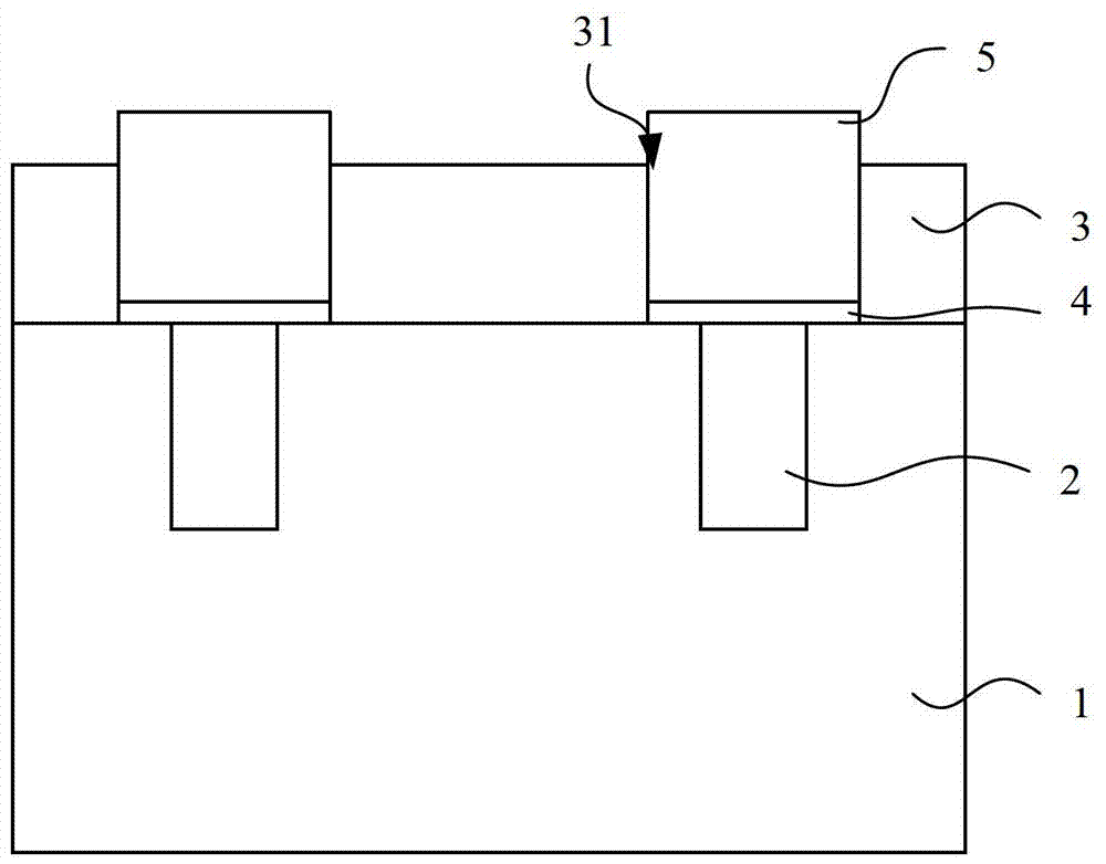
[0033] As mentioned in the background technology, there is a certain difference in the potential difference between the two ends of the metal pad in a wafer. At present, it can only be considered that the electrical properties of different regions will be different due to process problems. The specific reason is still unclear. After a lot of experiments, the inventor found that after adding titanium (Ti) and titanium nitride (TiN) between tantalum nitride (TaN) and metal pad aluminum as the isolation layer, the measured metal pad of the entire wafer The difference in potential difference is greatly reduced, thereby improving the detection pass rate.

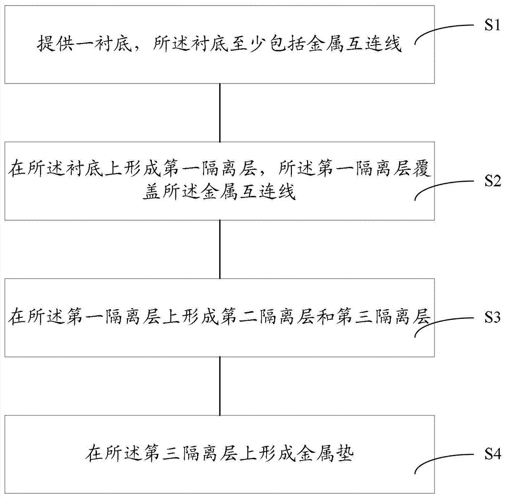
[0034] The method for forming the metal pad and the semiconductor structure provided by the present invention will be further described in detail below with reference to the accompanying drawings and specific embodiments. Advantages and features of the present invention will be apparent from the following description and claims. ...


PUM


Abstract

The invention discloses a metal pad forming method and a semiconductor structure. The method comprises the step that a first isolation layer TaN, a second isolation layer Ti and a third isolation layer TiN are formed on a substrate, wherein metal interconnection lines are covered with the first isolation layer TaN, the second isolation layer Ti and the third isolation layer TiN. The potential of one end and the potential of the other end of a metal pad of a whole wafer tend to be consistent and are even very small in difference, the degrees of dispersion is low when reliability is tested, and the yield can be improved easily. Moreover, because the isolation layers are added, gap fill becomes easier when the metal pad is formed, and the performance of devices can be improved easily.

Description

technical field [0001] The invention relates to the field of semiconductor manufacturing, in particular to a method for forming a metal pad and a semiconductor structure. Background technique [0002] The back-end process (BEOL) of integrated circuit manufacturing is mainly to form leads, which is usually done by forming metal pads. Considering that metal Cu is unstable, easy to oxidize and rust, and the requirements for resistance are not strict, most Metallic aluminum is used to realize the fabrication of the metal pad. [0003] current metal pads, which typically have features such as figure 1 The structure shown: [0004] A substrate 1, the substrate 1 includes metal interconnection lines 2, a passivation layer 3 located on the substrate 1, the passivation layer 3 is formed with a through hole 31, and the through hole 31 is formed with The barrier layer 4 , the metal aluminum 5 is located on said barrier layer 4 . Considering that the metal interconnection 2 is usual...

Claims


Application Information

Patent Timeline
Patent Type & Authority Patents(China)
IPC IPC(8): H01L21/60H01L23/485
CPCH01L24/03H01L24/06H01L2224/02123H01L2224/0215H01L2224/03H01L2224/06
Inventor 郭晓清徐俊龚春雷吕乐周真
Owner SEMICON MFG INT (SHANGHAI) CORP
Why Eureka
Try Eureka