

Multilayer passivation anti-reflective coating of crystalline silicon cell and manufacturing method thereof
A crystalline silicon battery, passivation reduction technology, applied in circuits, electrical components, final product manufacturing, etc., can solve the problems of insignificant difference in refractive index, escape from silicon wafers, etc., to reduce the surface density of states and achieve good light transmittance , Improve the effect of short-wave response
- Summary
- Abstract
- Description
- Claims
- Application Information
AI Technical Summary
Problems solved by technology
Method used
Image

Examples
preparation example Construction
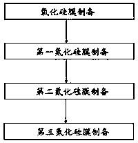
[0021] Such as figure 2 A multilayer passivation anti-reflection film for a crystalline silicon battery shown, its preparation method comprises the following steps:
[0022] (a) Cleaning, diffusion, and secondary cleaning of crystalline silicon cells;
[0023] (b) Use PECVD method to make silicon oxide film, wherein the flow rate of nitrogen gas is 15-25L / min, the flow rate of ammonia gas is 0.5-1L / min, the flow rate of laughing gas is 5-9L / min, and the flow rate of silane is 1-3L / min, Pressure 1-1.5Torr, electrode spacing 35-40mm, RF power 4-6kw, duration 10-15s, treatment temperature 300-400°C;
[0024] (c) Fabricate the first silicon nitride film on the silicon oxide film by PECVD method, wherein the flow rate of nitrogen gas is 15-25L / min, the flow rate of ammonia gas is 0.5-1L / min, the flow rate of silane is 2.5-3.5L / min, and the pressure 1-1.5Torr, the electrode spacing is 30-38mm, the RF power is 6-8kw, the duration is 8-15s, and the treatment temperature is 350-400°...
Embodiment 1
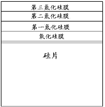
[0028] A multi-layer passivation anti-reflection film for a crystalline silicon battery. The passivation anti-reflection film is deposited on the N-type surface of a P-type crystalline silicon battery. The passivation anti-reflection film includes from bottom to top: a silicon oxide film , the first silicon nitride film, the second silicon nitride film, and the third silicon nitride film, wherein the thickness of the silicon oxide film is 20nm, the refractive index n1 is 1.5, the thickness of the first silicon nitride film is 10nm, and the refractive index n2 is 2.2, the thickness of the second silicon nitride film is 20 nm, the refractive index n3 is 2.1, the thickness of the third silicon nitride film is 35 nm, and the refractive index is 1.9.
[0029] Such as figure 2 A multilayer passivation anti-reflection film for a crystalline silicon battery shown, its preparation method comprises the following steps:
[0030] (a) Cleaning, diffusion, and secondary cleaning of the N-...
Embodiment 2
[0036] A multi-layer passivation anti-reflection film for a crystalline silicon battery. The passivation anti-reflection film is deposited on the N-type surface of a P-type crystalline silicon battery. The passivation anti-reflection film includes from bottom to top: a silicon oxide film , the first silicon nitride film, the second silicon nitride film, and the third silicon nitride film, wherein the thickness of the silicon oxide film is 15nm, the refractive index n1 is 1.6, the thickness of the first silicon nitride film is 15nm, and the refractive index n2 is 2.2, the thickness of the second silicon nitride film is 30nm, the refractive index n3 is 2.15, the thickness of the third silicon nitride film is 25nm, and the refractive index is 1.95.
[0037] Such as figure 2 A multilayer passivation anti-reflection film for a crystalline silicon battery shown, its preparation method comprises the following steps:
[0038] (a) Cleaning, diffusion, and secondary cleaning of the N-...
PUM
| Property | Measurement | Unit |
|---|---|---|
| Thickness | aaaaa | aaaaa |
| Thickness | aaaaa | aaaaa |
| Thickness | aaaaa | aaaaa |
Abstract
Description
Claims
Application Information