GaN-based LED epitaxial wafer with high external quantum efficiency and manufacturing method thereof

A technology of LED epitaxial wafers and external quantum efficiency, which is applied in the direction of electrical components, circuits, semiconductor devices, etc., can solve the problems of low external quantum efficiency of GaN-based LED epitaxial wafers, and improve external quantum efficiency, reduce source consumption, reduce The effect of growth time

Inactive Publication Date: 2014-12-24
AQUALITE CO LTD
View PDF5 Cites 19 Cited by
  • Summary
  • Abstract
  • Description
  • Claims
  • Application Information

AI Technical Summary

Problems solved by technology

[0004] In view of the above problems, the object of the present invention is to provide a GaN-based LED epitaxial wafer with high external quantum effici

Method used


Image

  • GaN-based LED epitaxial wafer with high external quantum efficiency and manufacturing method thereof

Examples


Embodiment Construction

[0017] In order to make the object, technical solution and advantages of the present invention clearer, the present invention will be further described in detail below in conjunction with the accompanying drawings and embodiments. It should be understood that the specific embodiments described here are only used to explain the present invention, not to limit the present invention.

[0018] In order to illustrate the technical solutions of the present invention, specific examples are used below to illustrate.

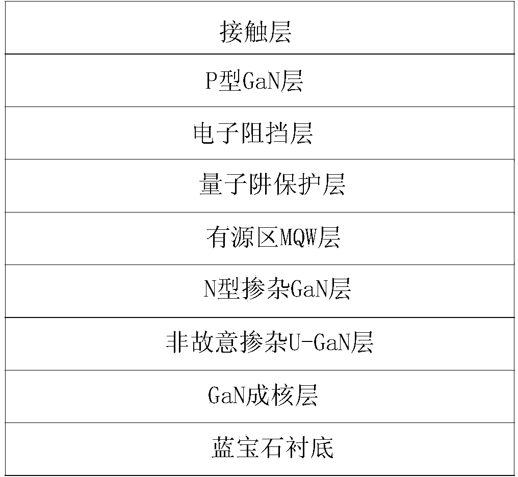
[0019] The embodiment of the present invention provides a high external quantum efficiency GaN-based LED epitaxial wafer and its growth method, such as figure 1 As shown, the epitaxial wafer is sequentially composed of sapphire substrate, GaN nucleation layer, unintentionally doped U-GaN layer, N-type doped GaN layer, active region MQW (Multi-Quantum Wells) layer, Quantum well protection layer, electron blocking layer, P-type GaN layer, contact layer. The specific prod...


PUM

PropertyMeasurementUnit
Thicknessaaaaaaaaaa
Growth temperatureaaaaaaaaaa
Thicknessaaaaaaaaaa

Abstract

The invention relates to the field of manufacturing of epitaxial wafers, and provides a GaN-based LED epitaxial wafer with high external quantum efficiency and a manufacturing method thereof. The method includes the steps that a GaN nuclearing layer, an involuntary doping U-GaN layer, an N-type doping GaN layer, an active area MQW layer, a quantum well protection layer, an electron blocking layer, a P-type GaN layer and a contact layer sequentially grow on a sapphire substrate; the electron blocking layer is an AlN layer or a superlattice layer formed by AlN and AlyInzGal-y-zN, y is larger than or equal to 0 and smaller than or equal to 1, z is larger than or equal to 0 and smaller than or equal to 1, the result of y plus z is larger than or equal to 0 and smaller than or equal to 1, growth temperature is 700-1200 DEG C and the thickness of the electron blocking layer is 3-100 nm. According to the GaN-based LED epitaxial wafer and the manufacturing method thereof, the thin AlN layer with high potential barriers can effectively performs the function of the electron blocking layer, the thickness of a whole P-layer structure can be reduced, the external quantum efficiency of an LED device can be obviously improved, growth time can be shortened, and production cost is reduced.

Description

technical field [0001] The invention belongs to the technical field of epitaxial wafer manufacturing, and in particular relates to a GaN-based LED epitaxial wafer with high external quantum efficiency and a manufacturing method thereof. Background technique [0002] Light Emitting Diode (LED, Light Emitting Diode)) has the advantages of small size, ruggedness, strong controllability of light-emitting band, high light efficiency, low heat loss, low light decay, energy saving, environmental protection, etc., and has been widely used in backlight, traffic indication Lights, car lights, street lights, toy decoration and other fields. The requirements for LEDs in application fields are getting higher and higher. Improving quality and reducing production costs are the goals that the LED industry has been pursuing. [0003] In the existing GaN-based LED epitaxial wafers, the electron blocking layer is grown by AlGaN, AlInGaN, etc., and the thickness of the entire P layer structure...

Claims


Application Information

Patent Timeline
IPC IPC(8): H01L33/04H01L33/00
CPCH01L33/007H01L33/06H01L33/145
Inventor 罗绍军艾常涛李鸿建李四明靳彩霞董志江
Owner AQUALITE CO LTD
Why Eureka
Try Eureka