
CMOS image sensor with high pixel and high frame rate and image collecting method

An image sensor and high frame rate technology, which is applied in the field of CMOS image sensor and image acquisition with high pixel and high frame rate, can solve problems such as limiting amplifier gain and bandwidth, complex timing, process influence, etc., to eliminate circuit offset and noise, The circuit structure is simple and the effect of improving the image quality

Active Publication Date: 2014-12-24
HARBIN ENG UNIV
View PDF3 Cites 12 Cited by
  • Summary
  • Abstract
  • Description
  • Claims
  • Application Information

AI Technical Summary

Problems solved by technology

At present, column-parallel ADCs generally use single-slope ADCs or cyclic ADCs. However, single-slope ADCs need 2 N clock cycles, limiting the speed increase; cyclic ADCs require very accurate amplifiers, resulting in higher power consumption
Sigma-Selta (ΣΔ) is a high-precision ADC commonly used in audio and video signal fields, but its complex timing and high power consumption limit its application in CMOS image sensors
In recent years, a ΣΔ ADC with a simple Class-C structure inverter as an operational amplifier has appeared, which has achieved lower power consumption, but the simple Class-C structure inverter used is seriously affected by the process, and the linearity The small gain range seriously limits the gain and bandwidth of the amplifier, and also limits the further improvement of the pixel array and frame rate in the CMOS image sensor it is applied to

Method used


Image

  • CMOS image sensor with high pixel and high frame rate and image collecting method
  • CMOS image sensor with high pixel and high frame rate and image collecting method
  • CMOS image sensor with high pixel and high frame rate and image collecting method

Examples


Embodiment Construction

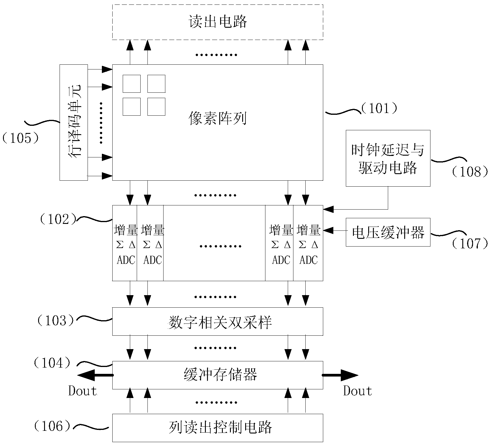
[0023] Such as figure 1 As shown, the CMOS image sensor of the present invention includes a pixel array section 101, an incremental ΣΔADC array section 102, a digital correlated double sampling section 103, and a buffer memory section 104 connected in sequence, and also includes a row decoding unit section 105, a row decoding unit section The signal output terminal of 105 is connected to the control terminal of the pixel array part (101), and also includes a column readout control circuit 106, the signal output terminal of the column readout control circuit 106 is connected to the control terminal of the buffer memory part, and the incremental ΣΔADC array part 102 is connected to There is a voltage buffer 107 and a clock delay and driver circuit 108 .

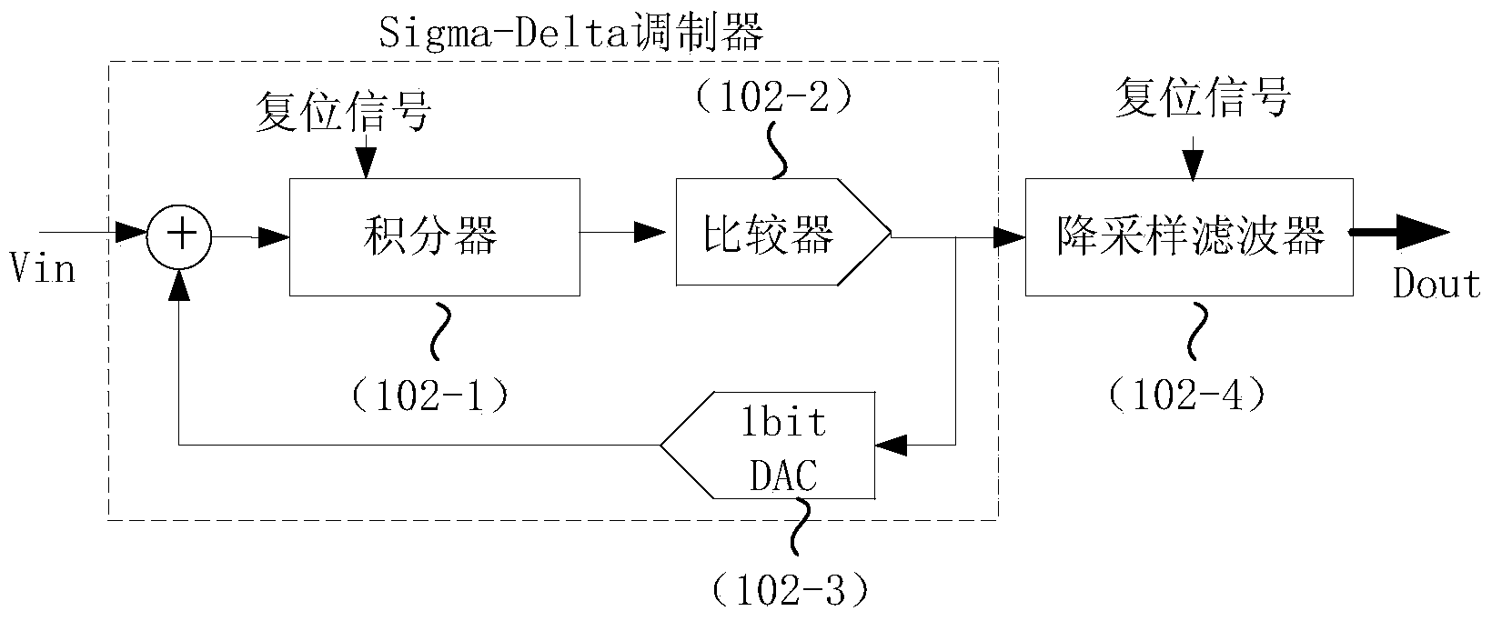
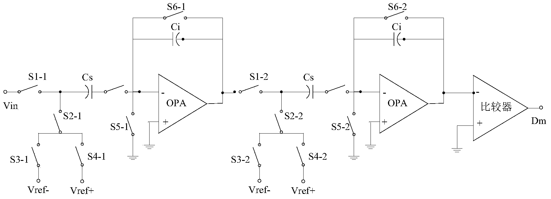
[0024] Such as figure 2 As shown, the incremental ΣΔADC is composed of an integrator 102-1, a comparator 102-2, a 1bit DAC 102-3 and a downsampling digital filter 102-4. This ΣΔ ADC is different from the traditional ΣΔ ADC. ...


PUM


Abstract

The invention relates to a CMOS image sensor with the high pixel and the high frame rate and an image collecting method. The CMOS image sensor comprises a pixel array part (101), an increment sigma delta DC array part (102), a digital correlation double-sampling part (103) and a buffer storage part (104) and further comprises a row coding unit part (105) and a column reading control circuit (106), wherein the pixel array part (101), the increment sigma delta DC array part (102), the digital correlation double-sampling part (103) and the buffer storage part (104) are sequentially connected, the signal output end of the row coding unit part (105) is connected with the control end of the pixel array part (101), the signal output end of the column reading control circuit (106) is connected with the control end of the buffer storage part, and the increment sigma delta DC array part (102) is connected with a voltage buffer (107) and a clock delaying and driving circuit (108).

Description

technical field [0001] The invention relates to a CMOS image sensor with high pixel and high frame rate and an image acquisition method. Background technique [0002] The image sensor is the core component of digital image acquisition. It uses the photoelectric conversion effect of semiconductor materials to realize the capture of optical signals, conversion to electrical signals and post-processing. In the past two decades, charge-coupled device (CCD) image sensors have been dominating the image sensor market due to their advantages such as low fixed-pattern noise, low dark current, high sensitivity, and high quantum efficiency. However, compared with CCD image sensors, CMOS image sensors can adopt mature CMOS process technology, and can integrate sensitive cell arrays, analog, and digital systems on a single chip, which has the advantages of low power consumption, low cost, and high integration. Therefore, the current CMOS image sensor has occupied most of the low-end mar...

Claims


Application Information

Patent Timeline
IPC IPC(8): H04N5/374H04N5/378
Inventor 刘云涛邵雷高松松
Owner HARBIN ENG UNIV
Learn More