Chemical processing apparatus
A processing device and liquid medicine technology, which is applied in the manufacture of electrical components, semiconductor/solid-state devices, circuits, etc., can solve problems affecting product costs and reduce the amount of liquid medicine used, so as to increase yield, improve processing efficiency, and suppress defects Effect
- Summary
- Abstract
- Description
- Claims
- Application Information
AI Technical Summary
Problems solved by technology
Method used
Image

Examples
Embodiment approach 1
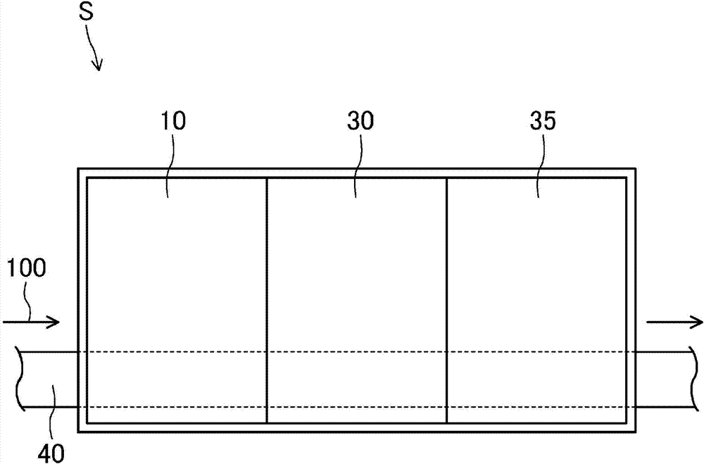
[0046] In this Embodiment 1, the etching processing apparatus S is demonstrated as an example of the chemical liquid processing apparatus of this invention.
[0047] The etching apparatus S of this embodiment is used to form patterns of wiring, electrodes, semiconductor layers, etc. on an insulating substrate as a base substrate, for example, when fabricating an active matrix substrate constituting a display panel such as a liquid crystal display device.
[0048] The substrate to be processed (object to be processed) W to be processed by the etching processing apparatus S is, for example, a rectangular flat glass substrate having a size of about 1000 mm to 3200 mm on one side. In addition, the processed substrate W may be the size of one display panel, or may be the size of mother substrates of multiple display panels.
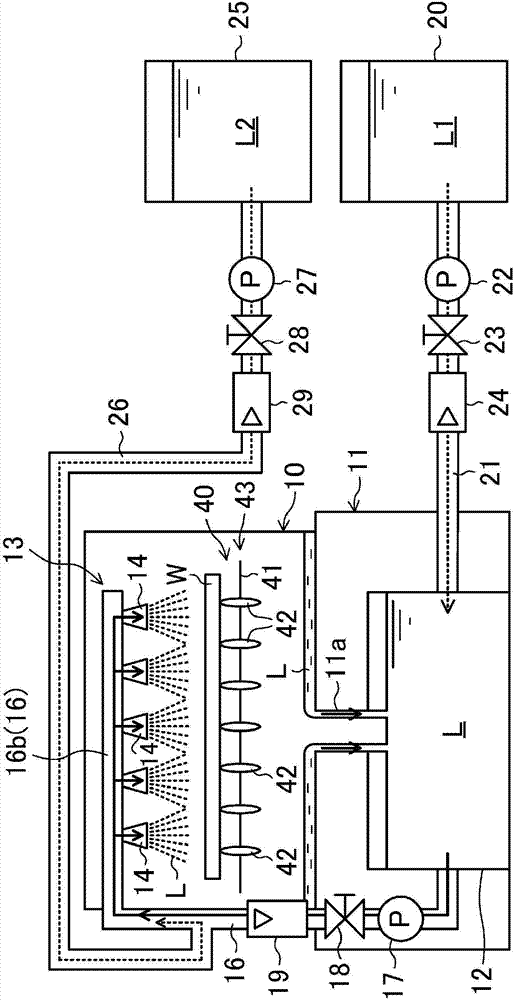
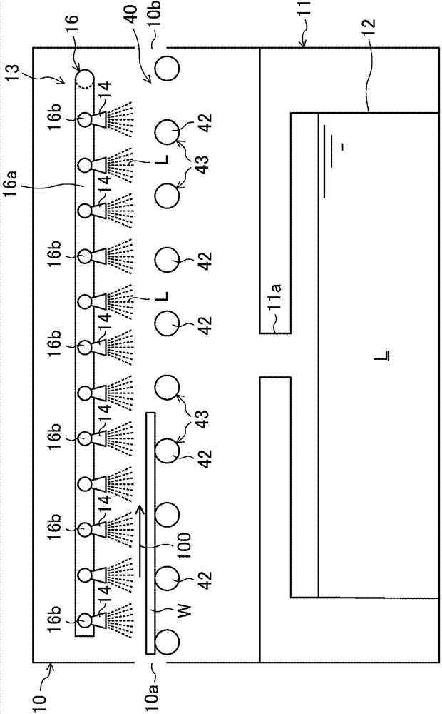
[0049] Configuration of etching processing device S
[0050] figure 1 It is a schematic diagram which shows the schematic structure of the etching proces...
Embodiment approach 2
[0094] Figure 5 It is a schematic diagram showing the internal structure of the etching treatment tank 10 of the second embodiment. In addition, in each of the following embodiments, the etching processing apparatus S has the same configuration as that of the first embodiment except for a part of configuration different from that of the first embodiment. Therefore, only the parts with different configurations will be described, and the same configuration will be transferred to Figure 1 ~ Figure 4 In the description of the first embodiment described above, the detailed description thereof is omitted.
[0095] The etching treatment tank 10 of the present embodiment is configured such that a loading detection sensor 50 for detecting the loading of the substrate W to be processed is provided above the loading port 10a side, and a detection sensor 50 is provided above the loading port 10b side. The carry-out detection sensor 52 that detects the carry-out of the processed substra...
Embodiment approach 3
[0102] The etching processing apparatus S of this Embodiment 3 is provided with the cleaning liquid tank (not shown) which stores a cleaning liquid in addition to the structure of Embodiment 1 mentioned above. This cleaning liquid tank is configured to replace the additive liquid tank 25 or to be connectable to the additive liquid piping 26 . As the cleaning solution, for example, pure water, ionized water, a solution containing a detergent, an acid solution for dissolving crystals of the L component of the etching solution, and the like are used.
[0103] Thus, for example, when it is desired to use a chemical solution different from the etching solution L used so far, or when it is desired to start using the processing device S after it has been stopped, the tank connected to the addition liquid piping 26 is removed from the Adding liquid tank 25 is connected with cleaning liquid tank instead, utilizes the driving of liquid supply pump 27 to make cleaning liquid flow from cl...
PUM
 Abstract
Description
Claims
Application Information
 - Generate Ideas
- Intellectual Property
- Life Sciences
- Materials
- Tech Scout
- Unparalleled Data Quality
- Higher Quality Content
- 60% Fewer Hallucinations
Browse by: Latest US Patents, China's latest patents, Technical Efficacy Thesaurus, Application Domain, Technology Topic, Popular Technical Reports.
© 2025 PatSnap. All rights reserved.Legal|Privacy policy|Modern Slavery Act Transparency Statement|Sitemap|About US| Contact US: help@patsnap.com