

Method for eliminating alloy surface bulge on junction area of top metal layer
A technology of top metal layer and bonding area, applied in electrical components, semiconductor/solid-state device manufacturing, circuits, etc., can solve the problem of affecting the contact and bonding of wires and bonding areas, affecting yield and chip electrical performance, increasing production costs, etc. problems, to achieve the effect of maintaining yield and electrical properties, reducing production costs, and improving adhesion
- Summary
- Abstract
- Description
- Claims
- Application Information
AI Technical Summary
Problems solved by technology
Method used
Image

Examples
Embodiment 1
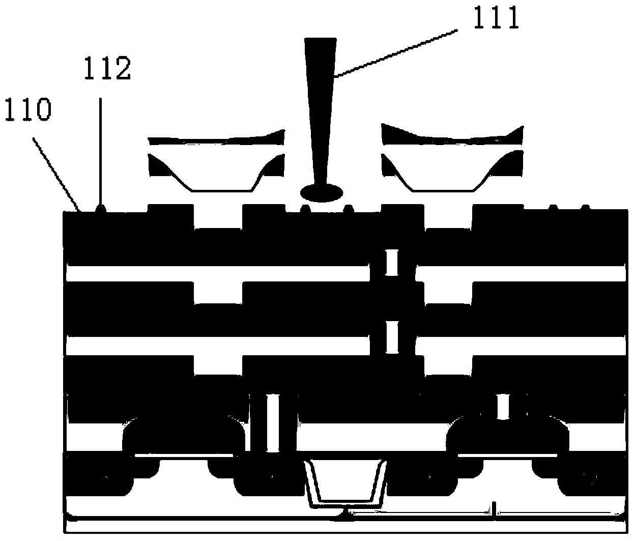
[0030] see figure 2 , Figure 3(a) and Figure 3(b) . Fig. 1 is the flowchart of the inventive method in a specific embodiment; Figure 3(a) —(b) is a schematic structural diagram corresponding to the processing flow of the present invention. As shown in Figure 1: as a preferred embodiment of the present invention, process step of the present invention is as follows:
[0031] Step 1 S210: forming a semiconductor device on the substrate and forming a metal interconnection layer on the semiconductor device. Such as Figure 3(a) As shown in and (b), three layers of metal interconnection layers are formed on the chip 210, which are the first metal interconnection layer 211, the second metal interconnection layer 212 and the topmost metal interconnection layer 213. The topmost layer The metal interconnection layer 213 is electrically connected to the lower second metal interconnection layer 212 and the first metal interconnection layer 211 through the metal plug 214 . Since...
Embodiment 2
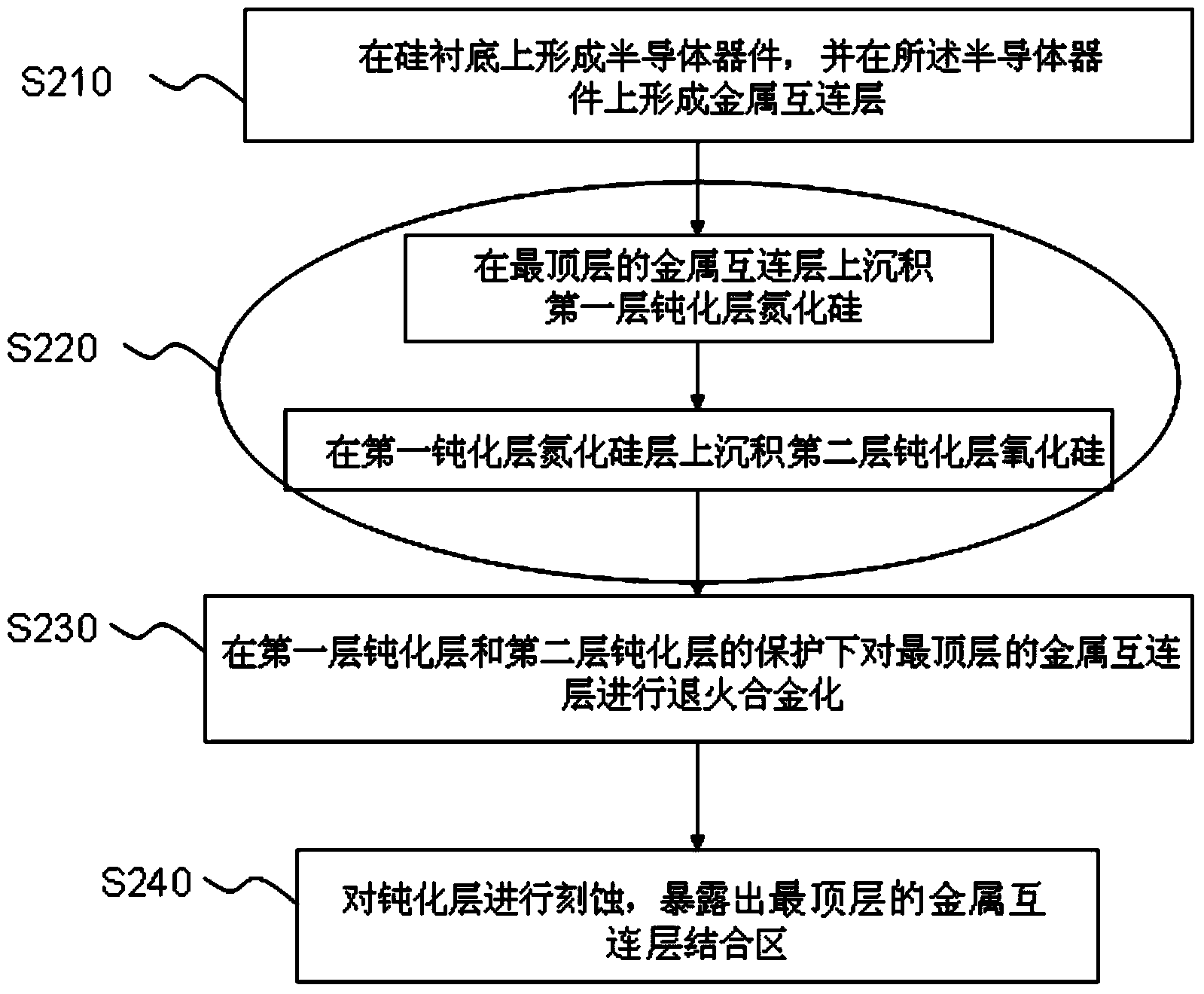
[0037] see Figure 4 , which is a flow chart of the method of the present invention in another specific embodiment. Such as Figure 4 As shown, as another preferred embodiment of the present invention, it includes the following steps:
[0038] Step 1 S410: forming a semiconductor device on the substrate, and forming a metal interconnection layer on the semiconductor device;
[0039] Step 2 S420: Deposit two passivation layers as protective layers on the topmost metal interconnection layer, the first passivation layer is silicon nitride, and the second passivation layer is silicon oxide, wherein the annealed alloy The oxidation is carried out after the first passivation layer is made of silicon nitride and before the second passivation layer of silicon oxide is deposited.
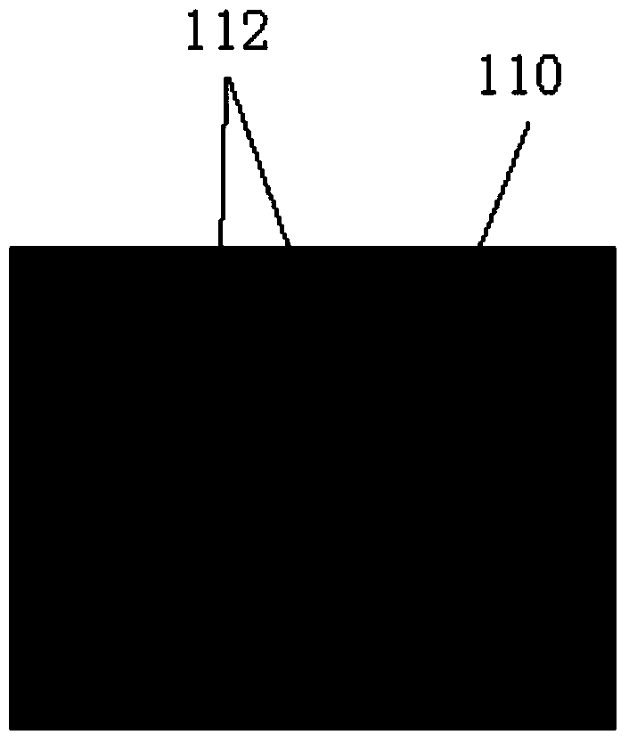
[0040] Step 3 S430: Etching the passivation layer to expose the bonding area of the topmost metal interconnection layer.
[0041] In this embodiment, except that the annealing and alloying is performed...
PUM
| Property | Measurement | Unit |
|---|---|---|
| thickness | aaaaa | aaaaa |
| thickness | aaaaa | aaaaa |
Abstract
Description
Claims
Application Information