Low-temperature polycrystalline silicon thin film manufacturing method, low-temperature polycrystalline silicon thin film and related devices

A technology of low-temperature polysilicon and a manufacturing method, which is applied to low-temperature polysilicon thin film transistors, array substrates and display devices, low-temperature polysilicon thin films and their manufacturing fields, can solve the problems affecting the performance of thin film transistors, threshold voltage drift, etc., and achieve uniform grain size. , The effect of preventing threshold voltage drift and uniform temperature

Active Publication Date: 2014-12-31
BOE TECH GRP CO LTD
View PDF6 Cites 2 Cited by
  • Summary
  • Abstract
  • Description
  • Claims
  • Application Information

AI Technical Summary

Problems solved by technology

The threshold voltage of a thin film transistor is related to many factors, including the doping of the crystalline silicon layer of the base layer, the thickness of the dielectric, the gate material and the dielectric or the charge condition at the interface between the dielectric and the semiconductor, etc., wherein the movable alkali metal ions ( Na

Method used


Image

  • Low-temperature polycrystalline silicon thin film manufacturing method, low-temperature polycrystalline silicon thin film and related devices
  • Low-temperature polycrystalline silicon thin film manufacturing method, low-temperature polycrystalline silicon thin film and related devices
  • Low-temperature polycrystalline silicon thin film manufacturing method, low-temperature polycrystalline silicon thin film and related devices

Examples


Embodiment Construction

[0038] In order to make the technical problems, technical solutions and advantages to be solved by the embodiments of the present invention clearer, the following will describe in detail with reference to the drawings and specific embodiments.

[0039] Embodiments of the present invention provide a low-temperature polysilicon thin film and a manufacturing method thereof, a low-temperature polysilicon thin-film transistor, an array substrate, and a display device, which can reduce alkali metal ions in the low-temperature polysilicon thin film, thereby effectively preventing threshold voltage drift of the low-temperature polysilicon thin-film transistor.

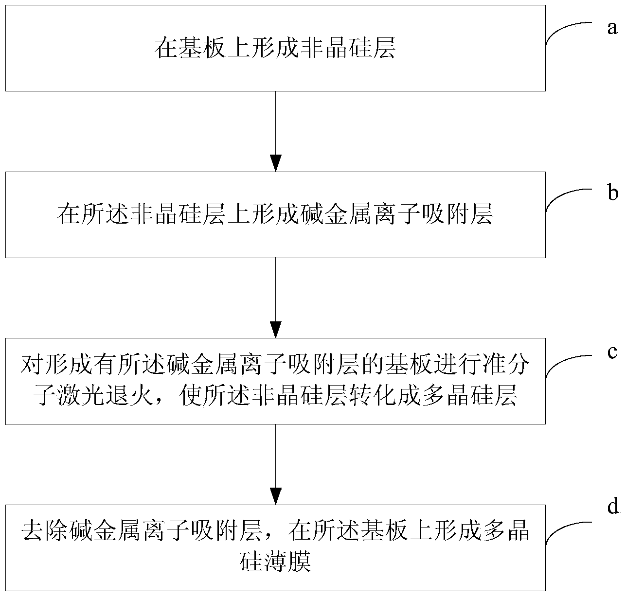
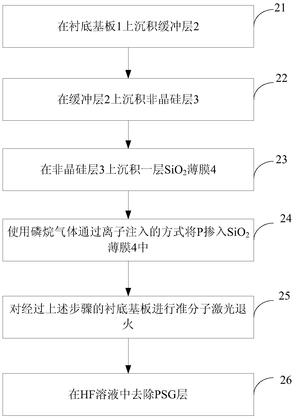
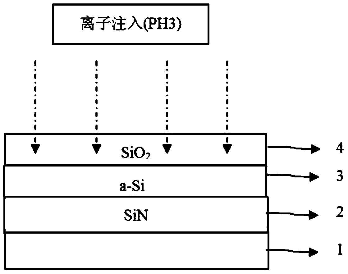
[0040] Embodiments of the present invention provide a method for manufacturing a low-temperature polysilicon film, such as figure 1 As shown, this embodiment includes:

[0041] Step a: forming an amorphous silicon layer on the substrate;

[0042] Step b: forming an alkali metal ion adsorption layer on the amorphous silicon la...


PUM

PropertyMeasurementUnit
Thicknessaaaaaaaaaa
Thicknessaaaaaaaaaa

Abstract

The invention provides a low-temperature polycrystalline silicon thin film manufacturing method, a low-temperature polycrystalline silicon thin film and related devices and belongs to the field of display panel manufacturing. The low-temperature polycrystalline silicon thin film manufacturing method comprises the following steps: forming an amorphous silicon layer on a substrate; forming an alkali metal ion adsorption layer on the amorphous silicon layer; conducting quasi-molecular laser annealing on the substrate on which the alkali metal ion adsorption layer is formed to convert the amorphous silicon layer into a polycrystalline silicon layer; removing the alkali metal ion adsorption layer to form a polycrystalline silicon thin film on the substrate. According to the technical scheme provided by the invention, alkali metal ions in the low-temperature polycrystalline silicon thin film can be reduced, so that the threshold voltage drift of a low-temperature polycrystalline silicon thin film transistor is effectively prevented.

Description

technical field [0001] The invention relates to the field of display panel manufacturing, in particular to a low-temperature polysilicon thin film and a manufacturing method thereof, a low-temperature polysilicon thin film transistor, an array substrate and a display device. Background technique [0002] Organic light-emitting display (OLED) has attracted much attention due to its many advantages such as self-illumination, fast response, thinness, low power consumption and flexible display, and is considered to be the next generation of flat panel display technology. At present, OLED technology has been gradually applied to various electronic products, among which the active matrix organic light-emitting display (AMOLED) is famous for its advantages of high image quality, short response time of moving images, low power consumption, wide viewing angle and ultra-light and ultra-thin. Become the main trend of OLED development. [0003] At present, polysilicon thin film transis...

Claims


Application Information

Patent Timeline
IPC IPC(8): H01L51/56H01L51/52
CPCH10K71/10H10K71/421H10K50/30H01L29/786
Inventor 张慧娟刘建宏
Owner BOE TECH GRP CO LTD
Why Eureka
Try Eureka