LDMOS device and forming method thereof

A device and doping type technology, applied in the direction of semiconductor devices, semiconductor/solid-state device manufacturing, electrical components, etc., to achieve the effect of constant breakdown voltage or small change, reduced point voltage, and large drive current

Inactive Publication Date: 2015-01-14
SEMICON MFG INT (SHANGHAI) CORP
View PDF4 Cites 5 Cited by
  • Summary
  • Abstract
  • Description
  • Claims
  • Application Information

AI Technical Summary

Problems solved by technology

[0005] The larger breakdown voltage and larger driving current make the LDMOS device have better switching characteristics and

Method used


Image

  • LDMOS device and forming method thereof
  • LDMOS device and forming method thereof
  • LDMOS device and forming method thereof

Examples


Embodiment Construction

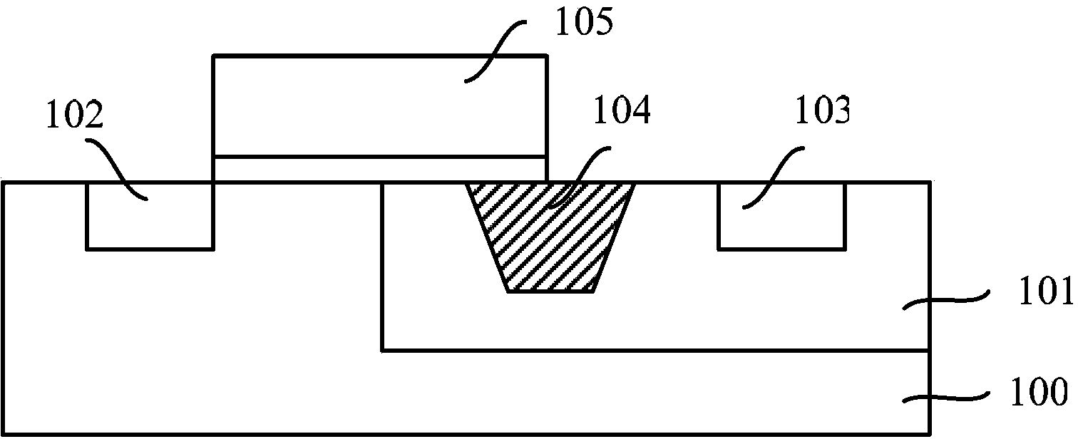
[0033] Please refer to figure 1 , in the production of existing LDMOS devices, in order to make the LDMOS device have a higher breakdown voltage, one of the ways is to form a shallow trench isolation structure 104 in the N-type drift region 101, and another way is to reduce the N The doping concentration of the type drift region 101 (or low doping concentration), but the above two methods will increase the on-resistance (equivalent on-resistance) between the source region 102 and the drain region 103 of the LDMOS device. Large, when the LDMOS device is working, when a certain operating voltage is applied to the source region 102 and the drain region 103, the driving circuit between the source region 102 and the drain region 103 will be reduced, that is, when the above method increases the driving voltage of the LDMOS device , the driving current of the LDMOS device under the same source-drain operating voltage will be correspondingly reduced, which is not conducive to the impr...


PUM

PropertyMeasurementUnit
Thicknessaaaaaaaaaa

Abstract

The invention discloses an LDMOS device and a forming method thereof. The LDMOS device comprises a semiconductor substrate, a drift region, a shallow trench isolation structure, a doping layer, a gate structure, a source region and a drain region. A well region is located in the semiconductor substrate. The drift region is located in the well region, and the doping type of the drift region is opposite to the doping type of the well region. The shallow trench isolation structure is placed in the drift region, and the depth of the shallow trench isolation structure is smaller than the depth of the drift region. The doping layer is placed at the bottom of the shallow trench isolation structure, and the doping type of the doping layer is opposite to the doping type of the drift region. The gate structure is placed on the semiconductor substrate, one end of the gate structure extends to the position above the well region, and the other end of the gate structure extends to the position above the shallow trench isolation structure. The source region is located in the well region on one side of the gate structure, and the drain region is located in the drift region on the other side of the gate structure. The breakdown voltage of the LDMOS device is kept unchanged, and meanwhile drive currents are increased.

Description

technical field [0001] The invention relates to the field of semiconductor manufacturing, in particular to an LDMOS device and a forming method thereof. Background technique [0002] Power field effect transistors mainly include two types: vertical double-diffused field effect transistor VDMOS (Vertical Double-Diffused MOSFET) and lateral double-diffused field effect transistor LDMOS (Lateral Double-Diffused MOSFET). Among them, compared with the vertical double diffused field effect transistor VDMOS, the lateral double diffused field effect transistor LDMOS has many advantages, for example, the latter has better thermal stability and frequency stability, higher gain and durability, lower Feedback capacitance and thermal resistance, as well as constant input impedance and simpler bias current circuit. [0003] Drive current (Ion) and breakdown voltage BV (Breakdown Voltage) are two important parameters to measure the performance of LDMOS devices. Among them, the driving cu...

Claims


Application Information

Patent Timeline
IPC IPC(8): H01L21/336H01L29/78H01L29/06
CPCH01L29/7835H01L29/063H01L29/0653H01L29/66689H01L29/7816
Inventor 孙光宇宋化龙
Owner SEMICON MFG INT (SHANGHAI) CORP
Why Eureka
Try Eureka