Three-mesa p-Pi-n structured III-nitride semiconductor avalanche photodetector and preparation method thereof

A technology of nitride semiconductor and avalanche photoelectricity, which is applied in the field of detectors, can solve the problems of large leakage current and edge breakdown, and achieve the effects of reducing strength, preventing premature breakdown, and simple manufacturing process

Inactive Publication Date: 2015-01-14
SUN YAT SEN UNIV
View PDF3 Cites 22 Cited by
  • Summary
  • Abstract
  • Description
  • Claims
  • Application Information

AI Technical Summary

Problems solved by technology

[0011] In order to overcome at least one defect described in the above-mentioned prior art, the present invention provides a three-mesa p-π-n structure Group III nitride semiconductor avalanche photodetector and its preparation method, the purpose of which is to further improve the leakage of traditional p-i-n structure devices. The current is large and the problem of early edge breakdown is prone to occur

Method used


Image

  • Three-mesa p-Pi-n structured III-nitride semiconductor avalanche photodetector and preparation method thereof
  • Three-mesa p-Pi-n structured III-nitride semiconductor avalanche photodetector and preparation method thereof
  • Three-mesa p-Pi-n structured III-nitride semiconductor avalanche photodetector and preparation method thereof

Examples


Embodiment Construction

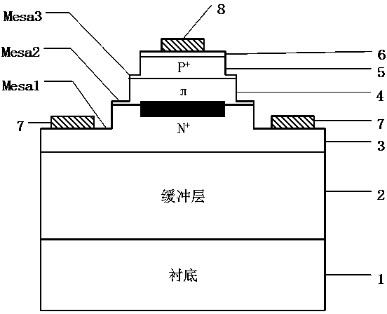
[0042] The accompanying drawings are for illustrative purposes only, and should not be construed as limitations on this patent; in order to better illustrate this embodiment, certain components in the accompanying drawings will be omitted, enlarged or reduced, and do not represent the size of the actual product; for those skilled in the art It is understandable that some well-known structures and descriptions thereof may be omitted in the drawings. The positional relationship described in the drawings is for illustrative purposes only, and should not be construed as a limitation on this patent.

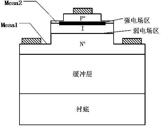
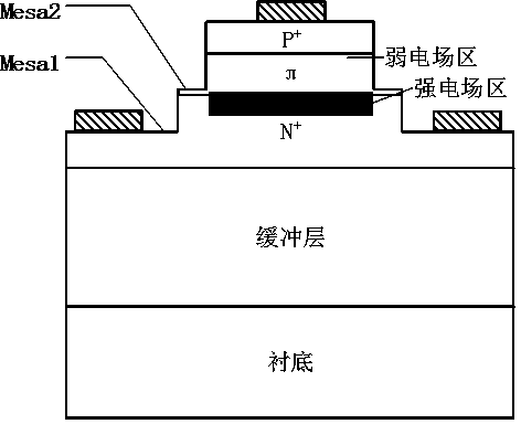
[0043] The present invention proposes to use the π active layer to replace the n-type high resistance layer (i-type layer) in the p-i-n structure to form a p-π-n structure (such as figure 2 ) method, which can effectively move down the position of the strong electric field region in the device (the strong electric field region in the p-π-n structure is located in the π-n junction dep...


PUM

PropertyMeasurementUnit
thicknessaaaaaaaaaa
thicknessaaaaaaaaaa
thicknessaaaaaaaaaa

Abstract

The invention relates to the technical field of detectors, in particular to a three-mesa p-Pi-n structured III-nitride semiconductor avalanche photodetector and a preparation method of the three-mesa p-Pi-n structured III-nitride semiconductor avalanche photodetector. The three-mesa p-Pi-n structured III-nitride semiconductor avalanche photodetector comprises a substrate, a buffer layer, an n-type doping nitride ohmic electrode contact layer, a Pi-type nitride active layer, a p-type doping nitride layer, a p-type heavy-doping nitride ohmic contact layer, n-type ohmic contact electrodes and a p-type ohmic contact electrode, wherein the buffer layer, the n-type doping nitride ohmic electrode contact layer, the Pi-type nitride active layer, the p-type doping nitride layer and the p-type heavy-doping nitride ohmic contact layer are sequentially grown on the substrate through epitaxial growth methods such as a molecular beam epitaxial method or an organometallic chemical vapor deposition epitaxial method; the n-type ohmic contact electrodes are manufactured on the n-type layer, and the p-type ohmic contact electrode is manufactured on the p-type layer. The three-mesa p-Pi-n structured III-nitride semiconductor avalanche photodetector can solve the problems that a traditional p-i-n structured device leaks a large number of currents and the edge of the traditional p-i-n structured device can be broken through easily in advance; moreover, a three-mesa structure conducts double-suppression protection on edge electric fields of a strong electric field region and a weak electric field region of a p-Pi-n structured device, so that the edge electric field is effectively prevented from being broken through in advance.

Description

technical field [0001] The present invention relates to the technical field of detectors, more specifically, to a three-mesa p-π-n structure Group III nitride semiconductor avalanche photodetector and a preparation method thereof. Background technique [0002] With the rapid development of information technology, ultraviolet detection technology plays an increasingly important role in the field of modern photoelectric information detection. At present, ultraviolet detectors have a wide range of application requirements in military or civilian fields such as flame detection, environmental monitoring, space optical communications, missile early warning systems, and quantum communications. Group III nitride semiconductors represented by GaN-based materials (including their binary compounds GaN, InN, and AlN, ternary compounds InGaN, AlGaN, and AlInN, and quaternary compounds AlInGaN) have large band gaps, direct band gaps, and electron migration. High efficiency, high breakdow...

Claims


Application Information

Patent Timeline
Patent Type & Authority Applications(China)
IPC IPC(8): H01L31/107H01L31/18H01L31/0352
CPCH01L31/035209H01L31/107H01L31/1856Y02P70/50
Inventor 江灏唐韶吉谭维
Owner SUN YAT SEN UNIV
Why Eureka
Try Eureka