Junction barrier Schottky diode with composite dielectric layer structure

A technology of junction barrier Schottky and composite dielectric, which is applied in the field of junction barrier Schottky diodes, can solve the problems that the breakdown voltage cannot reach the limit of GaN materials, the reverse leakage current is low, and the difficulty of increasing production is achieved. Avoid the Schottky barrier lowering effect, reduce the reverse leakage current, and optimize the effect of electric field distribution

Active Publication Date: 2017-11-24
UNIV OF ELECTRONICS SCI & TECH OF CHINA
View PDF3 Cites 2 Cited by
  • Summary
  • Abstract
  • Description
  • Claims
  • Application Information

AI Technical Summary

Problems solved by technology

However, the yield of large-area devices remains low due to material limitations
In 2011, Nomoto K et al published an article "Over 1.0kV GaN p-n Junction diodes on free-standing GaNsubstrates" ("Over 1000V GaN p-n junction diodes on GaN-based substrates"), which disclosed a method by using GaN-based substrates The GaN p-n junction diode made by field plate technology has a breakdown voltage of about 1000V and a reverse leakage current of 10 -9 A, but the junction termination technology such as field plate increases the complexity of the process, and the breakdown voltage of the p-n junction diode is small
In 2015, Tanaka N and others published an article: "A vertical GaN Schottky barrier diode on a free-standing GaN substrate with blocking voltage of 790V" ("Vertical GaN Schottky barrier diode based on GaN substrate with a breakdown voltage of 790V" ), which discloses a GaN SBD using field plate technology, the application of this technology makes its breakdown voltage reach 790V, and the forward current is about 50A, but there is still a defect of large reverse leakage current, and the field plate Isojunction terminal technology also increases the difficulty of production
Therefore, after the thickness of the N-type material layer reaches a certain value, the width of the depletion region of the N-type material layer reaches saturation during breakdown, and the breakdown voltage of the device also reaches saturation, which will limit the high-voltage application of GaN JBS; The strength of the longitudinal electric field formed from the anode to the cathode in the material layer will gradually decrease as the distance from the P-type doped region and the N-type material layer forms a PN junction interface. Integral on , and the ever-decreasing vertical electric field strength makes the breakdown voltage of the device unable to reach the limit of the GaN material, therefore, the high withstand voltage advantage of the GaN-based device cannot be fully utilized
In 2017, Koehler AD and others used JTE technology in the article "Vertical GaN Junction Barrier Schottky Diodes" ("Vertical GaN Junction Barrier Schottky Diodes"). The voltage is 610V, the reverse leakage current is low, which is smaller than that of SBD, but it is larger than the leakage current of PN junction diodes. In addition, the breakdown voltage of GaN JBS proposed in this article is small, and the structure size is large. In the material There are great difficulties in preparation, epitaxial growth and process manufacturing

Method used


Image

  • Junction barrier Schottky diode with composite dielectric layer structure
  • Junction barrier Schottky diode with composite dielectric layer structure
  • Junction barrier Schottky diode with composite dielectric layer structure

Examples


Embodiment 1

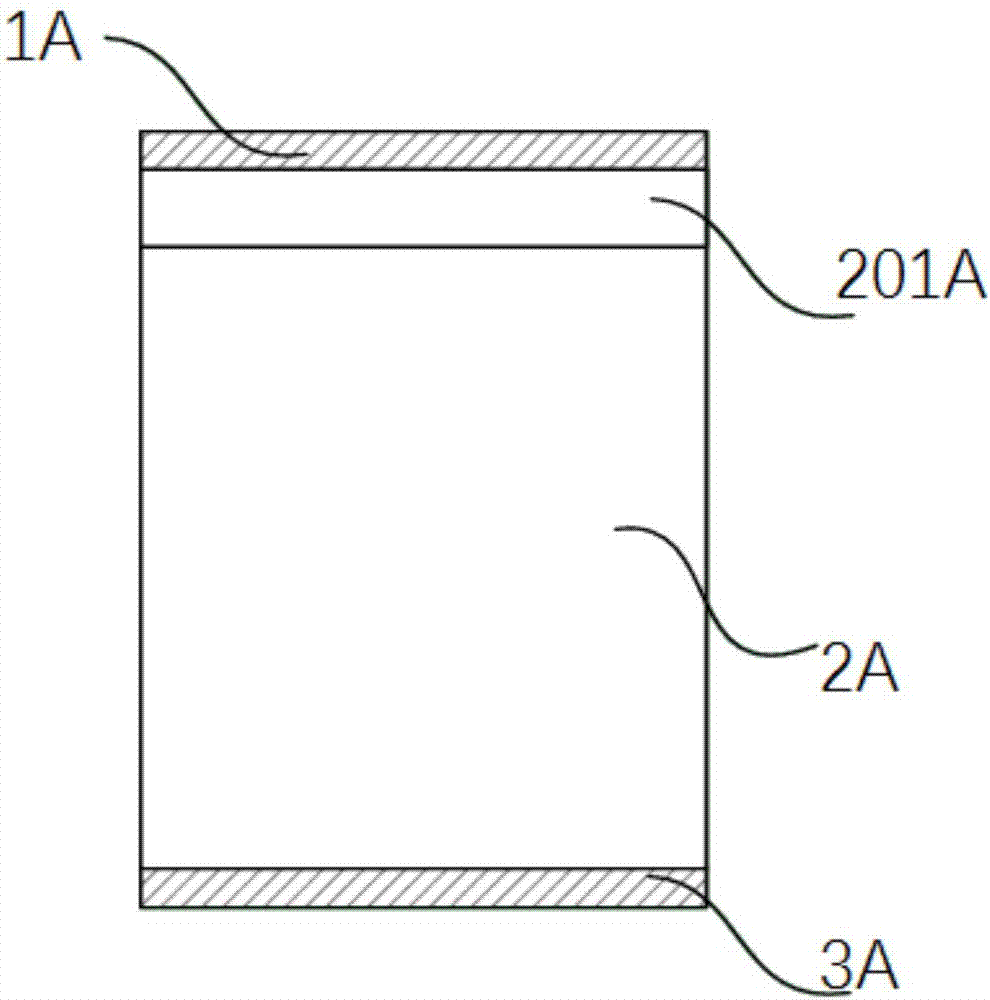
[0056] Such as Figure 4 As shown, the embodiment of the present invention provides a gallium nitride-based junction barrier Schottky diode with a composite dielectric layer structure (hereinafter abbreviated as HLKP JBS in this embodiment), and its cell structure sequentially includes from top to bottom: The metal anode 1, the N-type material layer 2 and the metal cathode 4, the upper layer of the N-type material layer 2 respectively has at least two mutually independent P-type doped regions 201; wherein, the metal anode 1 and the P-type doped region 201 An ohmic contact is formed on the surface, and both the metal anode 1 and the metal cathode 4 form Schottky contact with the N-type material layer 2; the doping concentration range of the N-type material layer 2 in this embodiment is 5×10 15 ~1×10 16 cm -3 ,

[0057] The present invention does not limit the shape of the N-type material layer 2, usually a rectangular parallelepiped. There are n mutually independent P-type doped re...

Embodiment 2

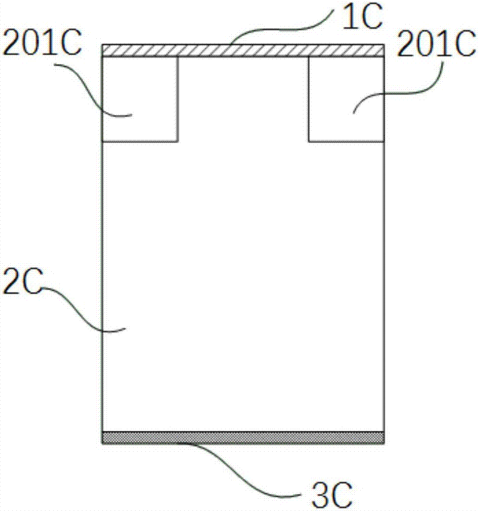
[0077] Combine Picture 10 with Picture 11 The present invention provides a gallium nitride-based junction barrier Schottky diode with a composite dielectric layer structure (hereinafter abbreviated as HLKP JBS in this embodiment). The device structure of this embodiment is in addition to the configuration and implementation of the composite dielectric layer 3. Except for the difference in Example 1, the rest of the structure is the same, so it will not be repeated here; however, in the device structure of this embodiment, the composite dielectric layer 3 is still symmetrically arranged on and in contact with the outer walls on both sides of the N-type material layer 2, which is the same as in Example 1. The difference is that the N-type material layer 2 and its P-type doped region 201 are only in contact with the same dielectric material. Specifically, the composite dielectric layer 3 on each side is composed of a third dielectric region 303 and a fourth dielectric region. 304...


PUM


Abstract

The invention provides a junction barrier Schottky diode with a composite dielectric layer structure, belonging to the field of power device technology. According to the junction barrier Schottky diode, composite dielectric layers that are formed by contacting high and low dielectric constants are separately arranged on outer walls of two sides of an N-type material layer, and a P-type gallium nitride region is arranged inside the N-type material layer to ensure that the distribution of a longitudinal electric field that is formed from the anode to the cathode is affected, the defect that the strength of the longitudinal electric field is greatly reduced existing in a traditional JBS device can be avoided, and meanwhile, the withstand voltage drop of the device caused by the junction edge electric field concentration effect can also be avoided, the early breakdown of the device can be prevented, and thus a high withstand voltage can be achieved on the basis of guaranteeing a small start voltage and a large conduction current. In addition, the junction barrier Schottky diode provided by the invention avoids the use of field ring structures and metal field plate structures, and thus the chip area can be reduced, the cost of the device can be reduced, and the reliability of the device can be improved.

Description

Technical field [0001] The invention belongs to the technical field of power devices, and specifically relates to a junction barrier Schottky diode with a composite dielectric layer structure. Background technique [0002] GaN power devices are attracting their rapid development in power device applications due to their high power, high frequency, high linearity, and high efficiency. Compared with the first generation semiconductor materials represented by silicon, the third generation semiconductor materials represented by gallium nitride have a wider band gap, a higher critical breakdown electric field, a higher melting point, and a higher electron mobility. Larger, higher limit operating temperature, which also means that GaN power devices can work at higher operating temperature, higher breakdown voltage and faster switching frequency. [0003] As we all know, the rectifier occupies an important position in the power application field, and the leakage and withstand voltage cap...

Claims


Application Information

Patent Timeline
Patent Type & Authority Applications(China)
IPC IPC(8): H01L29/06H01L29/872
CPCH01L29/0615H01L29/872
Inventor 杜江锋辛奇李振超白智元于奇
Owner UNIV OF ELECTRONICS SCI & TECH OF CHINA
Why Eureka
Try Eureka