Method for manufacturing grooved MOSFET device on basis of two-step microwave plasma oxidation

A technology of microwave plasma and manufacturing method, which is applied in the direction of semiconductor/solid-state device manufacturing, semiconductor devices, electrical components, etc., can solve the problems of poor stability of bottom gate oxide, inability to obtain forward characteristics, and abnormal operation of devices, etc. Achieve the effects of reducing electron defects, increasing effective mobility, and improving oxidation efficiency

Active Publication Date: 2018-11-06
INST OF MICROELECTRONICS CHINESE ACAD OF SCI
View PDF8 Cites 1 Cited by
  • Summary
  • Abstract
  • Description
  • Claims
  • Application Information

AI Technical Summary

Problems solved by technology

However, due to the thermal oxidation growth of SiO on the sidewall 2 The rate is several times that of the bottom oxidation rate, which makes the device unable to turn on when the gate voltage of the device reaches the maximum safe operating voltage of the gate oxide, and the channel region on the sidewall cannot be turned on because the gate voltage does not reach the threshold voltage, and the forward characteristic cannot be obtained. If the gate voltage continues to increase, the stability of the bottom gate oxide will deteriorate, causing premature breakdown of the bottom oxide layer, and the device cannot work normally.

Method used


Image

  • Method for manufacturing grooved MOSFET device on basis of two-step microwave plasma oxidation
  • Method for manufacturing grooved MOSFET device on basis of two-step microwave plasma oxidation
  • Method for manufacturing grooved MOSFET device on basis of two-step microwave plasma oxidation

Examples


Embodiment 1

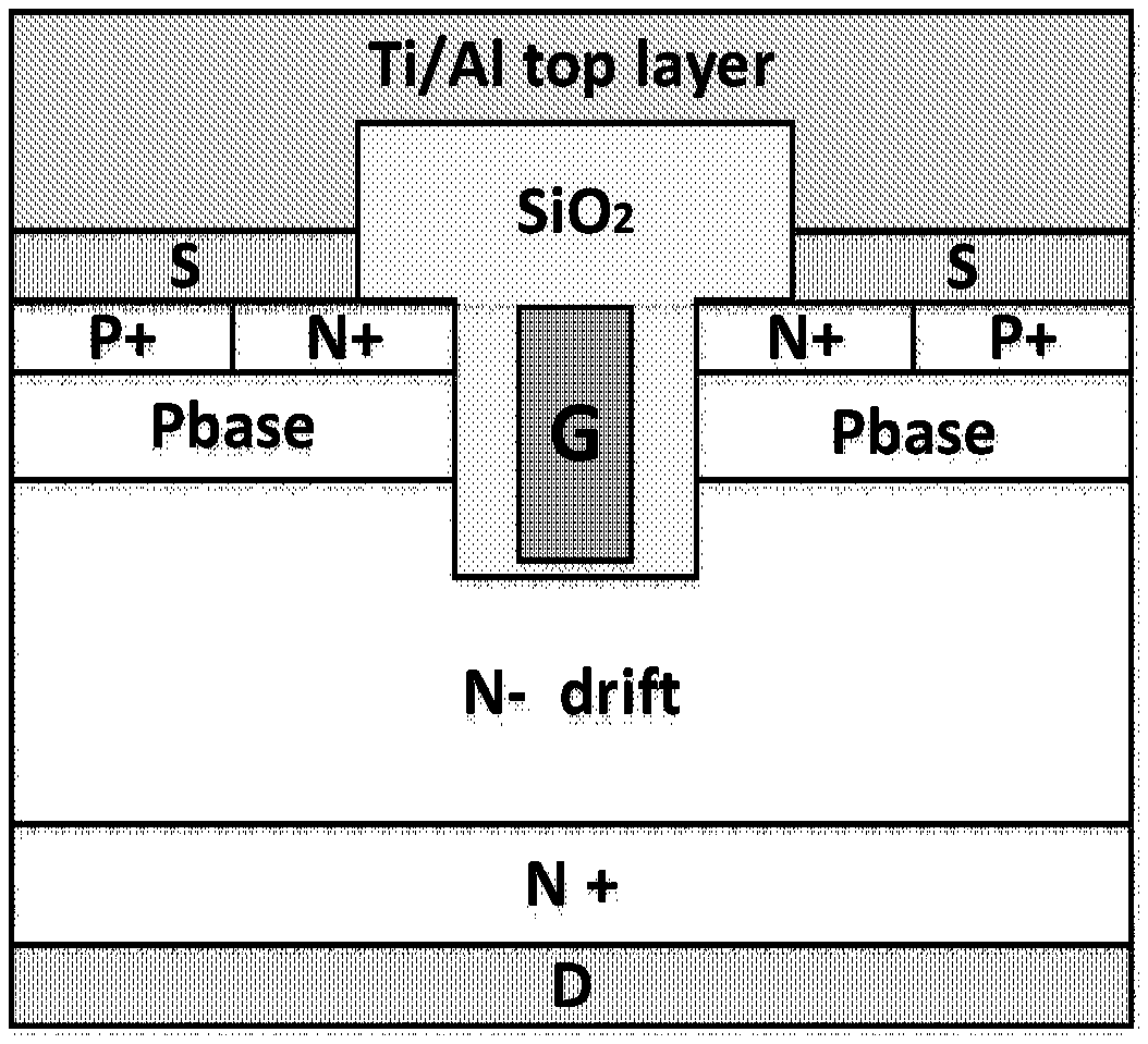
[0060] Such as Figure 4 As shown, the preparation method of the groove MOSFET device generally includes the following steps:

[0061] (1) cleaning the substrate;

[0062] (2) Forming a P-base implantation mask and ion implantation on the substrate;

[0063] (3) Form N-plus mask and ion implantation;

[0064] (4) Forming the P-base and removing the corresponding mask;

[0065] (5) Forming N-plus and removing the corresponding mask;

[0066] (6) Forming a P-plus mask and ion implantation;

[0067] (7) High temperature activation annealing;

[0068] (8) Forming P-plus and removing the corresponding mask;

[0069] (9) forming a groove gate etching mask;

[0070] (10) Groove gate etching;

[0071] (11) forming a groove gate oxide layer;

[0072] (12) making a polysilicon gate electrode;

[0073] (13) making the source electrode;

[0074] (14) making the drain electrode;

[0075] (15) making interlayer medium;

[0076] (16) Make the cover metal.

[0077] In this embod...


PUM


Abstract

The invention provides a method for manufacturing a grooved MOSFET device on the basis of two-step microwave plasma oxidation. The method comprises the step that after a grooved gate is etched, silicon carbide on the surface of the grooved gate is oxidized into silicon dioxide by means of microwave plasmas to form a grooved gate oxide layer. The grooved gate oxide layer is formed through the stepsthat the silicon carbide substrate after the grooved gate is etched is placed in a microwave plasma generation device; first oxygen-containing gas is introduced, the temperature of generated oxygen plasmas rises to the first temperature at a first temperature rising speed, and low-temperature plasma oxidation is conducted at the first temperature under the first pressure; the temperature of the oxygen plasmas rises to the second temperature at a second temperature rising speed, second oxygen-containing gas is introduced, and high-temperature plasma oxidation is conducted at the second temperature under the second pressure until silicon dioxide with the predetermined thickness is generated; and the oxygen-containing gas stops being introduced, and the reaction is finished. According to themethod, the oxidation efficiency of silicon carbide can be significantly improved, the interface quality is improved, and the uniform gate dielectric layer is formed.

Description

technical field [0001] The invention belongs to the technical field of semiconductors, and in particular relates to a method for manufacturing a groove MOSFET device based on two-step microwave plasma oxidation. Background technique [0002] Silicon carbide (SiC) is the third-generation semiconductor-wide bandgap semiconductor material. It has the advantages of large bandgap width, high critical breakdown field strength, and high thermal conductivity. It is an ideal material for making high-voltage and high-power semiconductor devices. SiC power Electronic devices are at the heart of next-generation high-efficiency power electronics technology. Compared with Si MOSFETs, SiC MOSFETs have smaller on-resistance, higher switching voltage, higher application frequency, and better temperature performance, and are especially suitable for power switching applications. The integrated manufacturing process of SiC MOSFET devices, especially the gate dielectric process, is a current re...

Claims


Application Information

Patent Timeline
Patent Type & Authority Applications(China)
IPC IPC(8): H01L21/336H01L21/28
CPCH01L21/049H01L29/66068H01L21/02236H01L21/02252H01L29/1608H01L29/7813H01L21/02164
Inventor 刘新宇汤益丹王盛凯白云杨成樾
Owner INST OF MICROELECTRONICS CHINESE ACAD OF SCI
Why Eureka
Try Eureka