Gallium nitride field effect transistor manufacturing method and gallium nitride field effect transistor

A gallium nitride field and manufacturing method technology, which is applied in semiconductor/solid-state device manufacturing, semiconductor devices, electrical components, etc., can solve problems such as poor voltage resistance, and achieve the effect of improving voltage resistance

Inactive Publication Date: 2017-10-03
PEKING UNIV +2
View PDF3 Cites 1 Cited by
  • Summary
  • Abstract
  • Description
  • Claims
  • Application Information

AI Technical Summary

Problems solved by technology

[0004] The invention provides a method for manufacturing a gallium nitride field effect transistor and a gallium nitride field effect transistor, so as to solve the problem of poor pressure resistance of the gallium nitride field effect transistor in the prior art

Method used


Image

  • Gallium nitride field effect transistor manufacturing method and gallium nitride field effect transistor
  • Gallium nitride field effect transistor manufacturing method and gallium nitride field effect transistor
  • Gallium nitride field effect transistor manufacturing method and gallium nitride field effect transistor

Examples


Embodiment 1

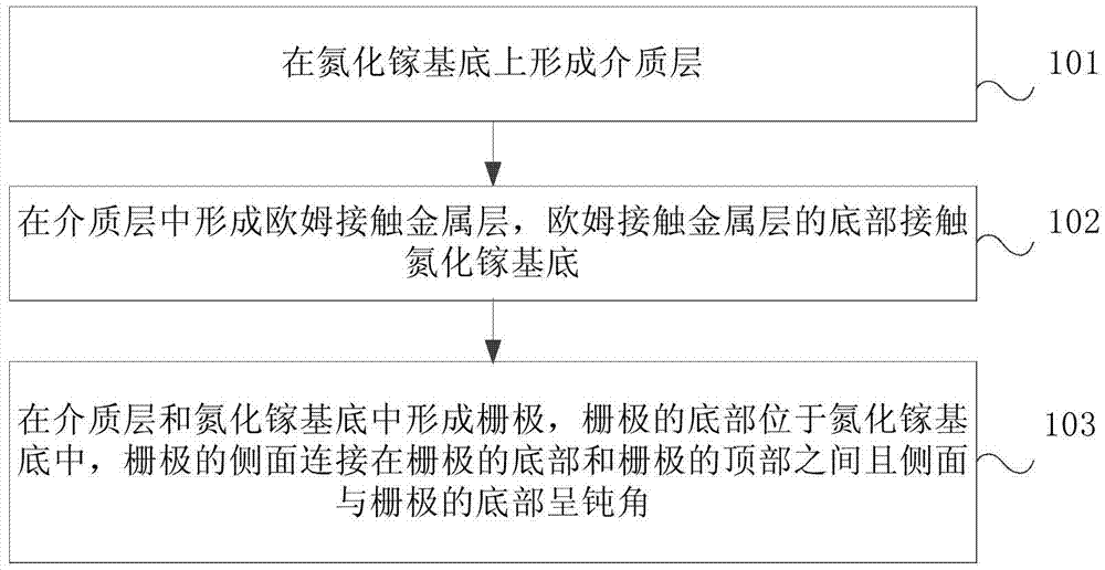
[0020] This embodiment provides a method for manufacturing a GaN field effect transistor, which is used for manufacturing a GaN field effect transistor.

[0021] like figure 1 As shown, is a schematic flow chart of the fabrication method of the eGaN field effect transistor according to the present embodiment. The fabrication method of the gallium nitride field effect transistor includes:

[0022] Step 101, forming a dielectric layer on a gallium nitride substrate.

[0023] The dielectric layer can be composed of one layer of material, or multiple layers of material, and this step can specifically be:

[0024] forming a passivation layer on the gallium nitride substrate;

[0025] An oxide layer is formed on the passivation layer.

[0026] The passivation layer of this embodiment can be Si 3 N 4 layer, the oxide layer may be a PETEOS (Plasma enhanced tetraethyl orthosilicate, plasma enhanced deposition of tetraethoxysilane) layer.

[0027] The gallium nitride substrate in...

example 2

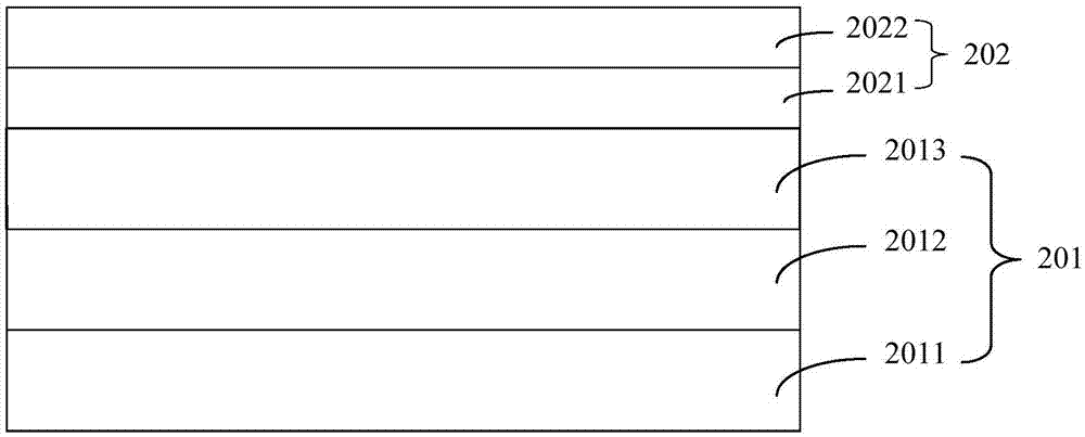
[0041] This embodiment provides a specific manufacturing method of a GaN field effect transistor manufacturing method. like Figures 2A to 2F Shown is a structural schematic diagram of each step in the manufacturing method of the eGaN field effect transistor according to the present embodiment.

[0042] like Figure 2A As shown, a dielectric layer 202 is formed on a GaN substrate 201 .

[0043] The gallium nitride substrate 201 includes a Si substrate 2011 , a GaN layer 2012 and an AlGaN layer 2013 which are sequentially formed from bottom to top. The dielectric layer 202 in this embodiment includes a passivation layer 2021 and an oxide layer 2022. Specifically, a layer of Si may be formed on the surface of the barrier layer of the AlGaN layer 2013. 3 N 4 layer as a passivation layer 2021, and the Si 3 N 4 A PETEOS layer is formed on the layer as the oxide layer 2022.

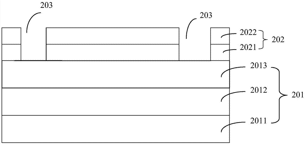
[0044] like Figure 2B As shown, an ohmic contact hole 203 is formed in the dielectric layer 202 to ex...

Embodiment 3

[0059] This embodiment provides a gallium nitride field effect transistor, which is specifically manufactured by the method of embodiment 1 or embodiment 2.

[0060] like Figure 2F As shown, the GaN field effect transistor of this embodiment includes a GaN substrate 201 , a dielectric layer 202 , an ohmic contact metal layer 205 and a gate 207 .

[0061] Wherein, the dielectric layer 202 is formed on the gallium nitride substrate 201; the ohmic contact metal layer 205 is formed in the dielectric layer 202, and the bottom of the ohmic contact metal layer 205 contacts the gallium nitride substrate 201; the gate 207 is formed in the dielectric layer 202, The bottom of the gate 207 is located in the gallium nitride substrate 201, the top 2071 of the gate 207 is higher than the dielectric layer 202 or flush with the dielectric layer 202, and the side 2073 of the gate 207 is connected to the bottom 2072 of the gate 207 and the gate 207 Between the top 2071 of the gate 207 and the ...


PUM


Abstract

The invention provides a manufacturing method of a gallium nitride field effect transistor and the gallium nitride field effect transistor. The method comprises the following steps: forming a dielectric layer on a gallium nitride substrate; forming an ohmic contact metal layer in the dielectric layer, wherein the bottom of the ohmic contact metal layer is in contact with the gallium nitride substrate; forming a grid electrode in the dielectric layer and the gallium nitride substrate, wherein the bottom of the grid electrode is located in the gallium nitride substrate, the side surface of the grid electrode is connected between the bottom of the grid electrode and the top of the grid electrode, and an obtuse angle is formed between the side surface and the bottom of the grid electrode. According to the manufacturing method of the gallium nitride field effect transistor, the voltage resistance of the gallium nitride field effect transistor can be improved.

Description

technical field [0001] The invention relates to semiconductor technology, in particular to a manufacturing method of a gallium nitride field effect transistor and a gallium nitride field effect transistor. Background technique [0002] Power devices featuring low power consumption and high speed have recently attracted a lot of attention as the need for efficient and complete power conversion circuits and systems has increased. GaN is the third generation wide bandgap semiconductor material, because of its large bandgap width (3.4eV), high electron saturation rate (2e 7 cm / s), high breakdown electric field (1e 10 V / cm-3e 10 V / cm), high thermal conductivity, corrosion resistance and radiation resistance, have strong advantages in high pressure, high frequency, high temperature, high power and radiation resistance environmental conditions, it is considered to be the research of short-wave optoelectronic devices and high voltage high voltage The best material for frequency h...

Claims


Application Information

Patent Timeline
Patent Type & Authority Applications(China)
IPC IPC(8): H01L21/335H01L21/28H01L29/772H01L29/423
CPCH01L29/66409H01L21/28H01L29/42316H01L29/772
Inventor 刘美华孙辉林信南陈建国
Owner PEKING UNIV
Why Eureka
Try Eureka