A kind of gan epitaxy process method

An epitaxial process and process technology, applied in chemical instruments and methods, sustainable manufacturing/processing, crystal growth, etc., can solve the problems of large differences in lattice constants, affecting the quality of GaN epitaxy, and large adaptability, and achieve relief Effects of lattice mismatch, improvement of epitaxial quality, and reduction of lattice defects

Active Publication Date: 2016-10-19
SHANGHAI HUAHONG GRACE SEMICON MFG CORP
View PDF5 Cites 0 Cited by
  • Summary
  • Abstract
  • Description
  • Claims
  • Application Information

AI Technical Summary

Problems solved by technology

However, the lattice constants of the buffer layer and Si differ greatly, and the degree of fit between the two is very large, which leads to more lattice defects in the buffer layer close to the Si substrate, and the lattice defects diffuse to the GaN epitaxial layer. layer (see figure 1 ), thus affecting the quality of GaN epitaxy

Method used


Image

  • A kind of gan epitaxy process method
  • A kind of gan epitaxy process method
  • A kind of gan epitaxy process method

Examples


Embodiment Construction

[0019] The present invention will be described in further detail below in conjunction with the accompanying drawings and embodiments.

[0020] Such as Figure 2-Figure 5 As shown, a GaN epitaxial process method of the present invention specifically includes the following steps:

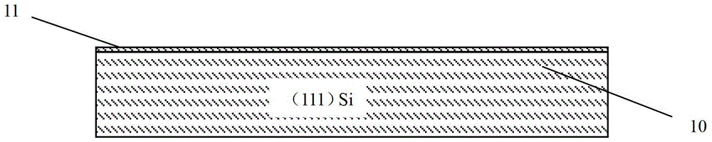
[0021] 1) if figure 2 As shown, Si is grown on a silicon substrate 10 with a crystal orientation of (111) (1-x-y) GexCy buffer layer 11; the surface crystal orientation of silicon substrate 10 is (111), Si (1-x-y) The GexCy buffer layer 11 satisfies: 8.2%≤x / y≤10.7%, and the thickness of the buffer layer 11 is 1-100nm. It is grown by vapor phase epitaxy or ultra-high vacuum chemical vapor deposition, the growth temperature is 500-1000 degrees Celsius, and the reaction gas source is SiH 4 or DCS (dichlorodihydrosilane), GeH 4 , SiH 3 CH 3 and H 2 .

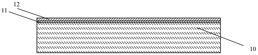
[0022] 2) if image 3 As shown, gradually reduce the Si (1-x-y) The content of Ge in the GexCy buffer layer 11 is until it is 0, thereby growin...


PUM

PropertyMeasurementUnit
thicknessaaaaaaaaaa
thicknessaaaaaaaaaa
thicknessaaaaaaaaaa

Abstract

The invention discloses a GaN epitaxial technological method, which comprises the following steps of: 1) growing an Si(1-x-y)GexCy buffer layer on a silicon substrate; 2) gradually decreasing the content of Ge in the Si(1-x-y)GexCy buffer layer to 0, thus obtaining an Si(1-x-y)GexCy and SiC buffer layer; 3) growing an SiC buffer layer on the Si(1-x-y)GexCy and SiC buffer layer; and 4) carrying out GaN epitaxial growth on the SiC buffer layer to form a GaN epitaxial layer. According to the method provided by the invention, buffer layers with gradually changing lattice constants are utilized to grow the high quality GaN epitaxial layer, and the method can prevent GaN defects and improve the quality of GaN epitaxy.

Description

technical field [0001] The invention belongs to the manufacturing process of semiconductor integrated circuits, and relates to an epitaxy process method, in particular to a GaN epitaxy process method. Background technique [0002] GaN is a wide bandgap semiconductor material, which has excellent physical and chemical properties, such as large bandgap width, high breakdown electric field strength, high saturation electron drift velocity, high thermal conductivity and strong radiation resistance, thermal conductivity and Large dielectric constant, stable chemical properties, etc., especially suitable for making semiconductor devices used in high-voltage, high-temperature, high-frequency, high-power, and strong-irradiation environments. Specifically, the band gap of GaN is larger than that of Si material, and the intrinsic carrier concentration is lower than that of Si, which determines that the limit operating temperature of GaN-based devices is higher than that of Si-based de...

Claims


Application Information

Patent Timeline
Patent Type & Authority Patents(China)
IPC IPC(8): C30B25/02C30B25/18C30B29/38H01L31/18
CPCY02P70/50
Inventor 刘继全
Owner SHANGHAI HUAHONG GRACE SEMICON MFG CORP
Why Eureka
Try Eureka