GeSn quantum well infrared illuminator with strain source

A technology of infrared luminescence and quantum wells, which is applied in semiconductor devices, electrical components, circuits, etc., can solve the problems of poor material quality and thermal stability, difficulty in wide-range bandgap adjustment, etc., and achieve the effect of rapid and efficient radiation recombination

Inactive Publication Date: 2015-01-21
CHONGQING UNIV
View PDF3 Cites 9 Cited by
  • Summary
  • Abstract
  • Description
  • Claims
  • Application Information

AI Technical Summary

Problems solved by technology

However, with the increase of Sn composition, the quality and thermal stability of the material will deteriorate, so it is difficult to adjust the band gap in a wide range by simply increasing the composition of Sn.

Method used


Image

  • GeSn quantum well infrared illuminator with strain source
  • GeSn quantum well infrared illuminator with strain source
  • GeSn quantum well infrared illuminator with strain source

Examples


Embodiment Construction

[0019] In order to understand the technical essence of the present invention more clearly, the structure and process realization of the present invention are described in detail below in conjunction with the accompanying drawings and embodiments:

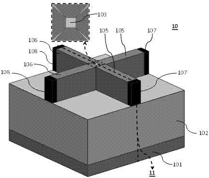
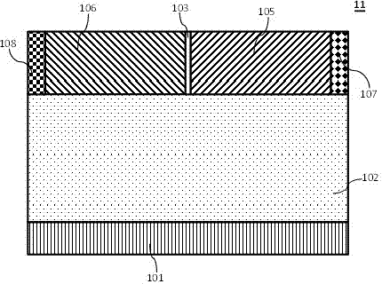
[0020] see figure 1 and figure 2 The shown GeSn quantum well infrared emitter with a strain source, which includes:

[0021] The active region 103 and the relaxed layer 102 , the active region 103 is located on the relaxed layer 102 . They use single crystal GeSn material, the general formula of the material is Ge 1-x sn x (0≤ x ≤0.25), if Ge can be used 0.93 sn 0.07 .

[0022] no + Type strainer 105 with p + Type strain source 106, distributed in pairs around the active region, using single crystal SiGe material, the general formula of the material is Si 1-x Ge x (0≤ x ≤0.4), if Si can be used 0.7 Ge 0.3 .

[0023] The two first electrodes 107 are connected to the strain source 105 .

[0024] The two second electr...


PUM


Abstract

The invention provides a GeSn quantum well infrared illuminator with a strain source. The structure is characterized in that a relaxation layer GeSn is arranged on a silicon substrate; strain source potential barriers n+ SiGe and p+ SiGe are arranged on the relaxation layer and grows at the peripheral region of an active region GeSn in pairs; and one end of the strain source potential barrier SiGe is a metal contact electrode. The lattice constant of the material of the strain source SiGe is smaller than that of the material of the active region GeSn, thereby forming single-axis compression strain along the z axis direction on the active region GeSn material, and forming a double-axis tensile strain along the xy plane; the strain state facilitates the GeSn material to change from an indirect band gap to a direct band gap; and through forming a heterojunction quantum well structure through the GeSn and the SiGe, fast and efficient radiative recombination of electron-hole is realized. The structure can limit electrons and holes in the well efficiently, thereby enlarging recombination rate of the electron and hole pairs, and improving luminous efficiency of an illuminator.

Description

technical field [0001] The invention relates to a GeSn quantum well infrared light emitter with a strain source. Background technique [0002] With the rapid development of optoelectronic integration technology and optical communication technology, infrared light-emitting devices with high efficiency and large-scale integration have become an urgent problem to be solved. GeSn alloy with novel properties is a new material that is expected to solve this problem. Theory and experiments show that GeSn has higher carrier mobility than pure Ge materials. Theoretical calculations show that by adjusting the composition of Sn in GeSn and changing the strain of the GeSn structure, the indirect bandgap structure of GeSn can be Γ point down (Physical Review B, vol. 75, pp. 045208, 2007). [0003] For the relaxed GeSn material, when the composition of Sn reaches 6.5%~11%, GeSn will become a direct bandgap ( E gΓ < E gL ) (Journal of Applied Physics, 113, 073707, 2013 and refere...

Claims


Application Information

Patent Timeline
Patent Type & Authority Applications(China)
IPC IPC(8): H01L33/06H01L33/34
CPCH01L33/06H01L33/34
Inventor 刘艳韩根全张庆芳王轶博
Owner CHONGQING UNIV
Why Eureka
Try Eureka