Vertical-cavity surface-emitting semiconductor laser

A vertical cavity surface emission and semiconductor technology, applied in the field of lasers, can solve the problems of low output power and poor stability of VCSEL, and achieve the effects of high power and high stability single-mode output, increased loss, and increased gain

Active Publication Date: 2015-01-21
吉光半导体科技有限公司
View PDF7 Cites 14 Cited by
  • Summary
  • Abstract
  • Description
  • Claims
  • Application Information

AI Technical Summary

Problems solved by technology

[0005] The purpose of the present invention is to provide a vertical cavity surface emitting semiconductor

Method used


Image

  • Vertical-cavity surface-emitting semiconductor laser
  • Vertical-cavity surface-emitting semiconductor laser
  • Vertical-cavity surface-emitting semiconductor laser

Examples


preparation example Construction

[0031] The preparation method of the above-mentioned vertical cavity surface emitting semiconductor laser comprises the following steps:

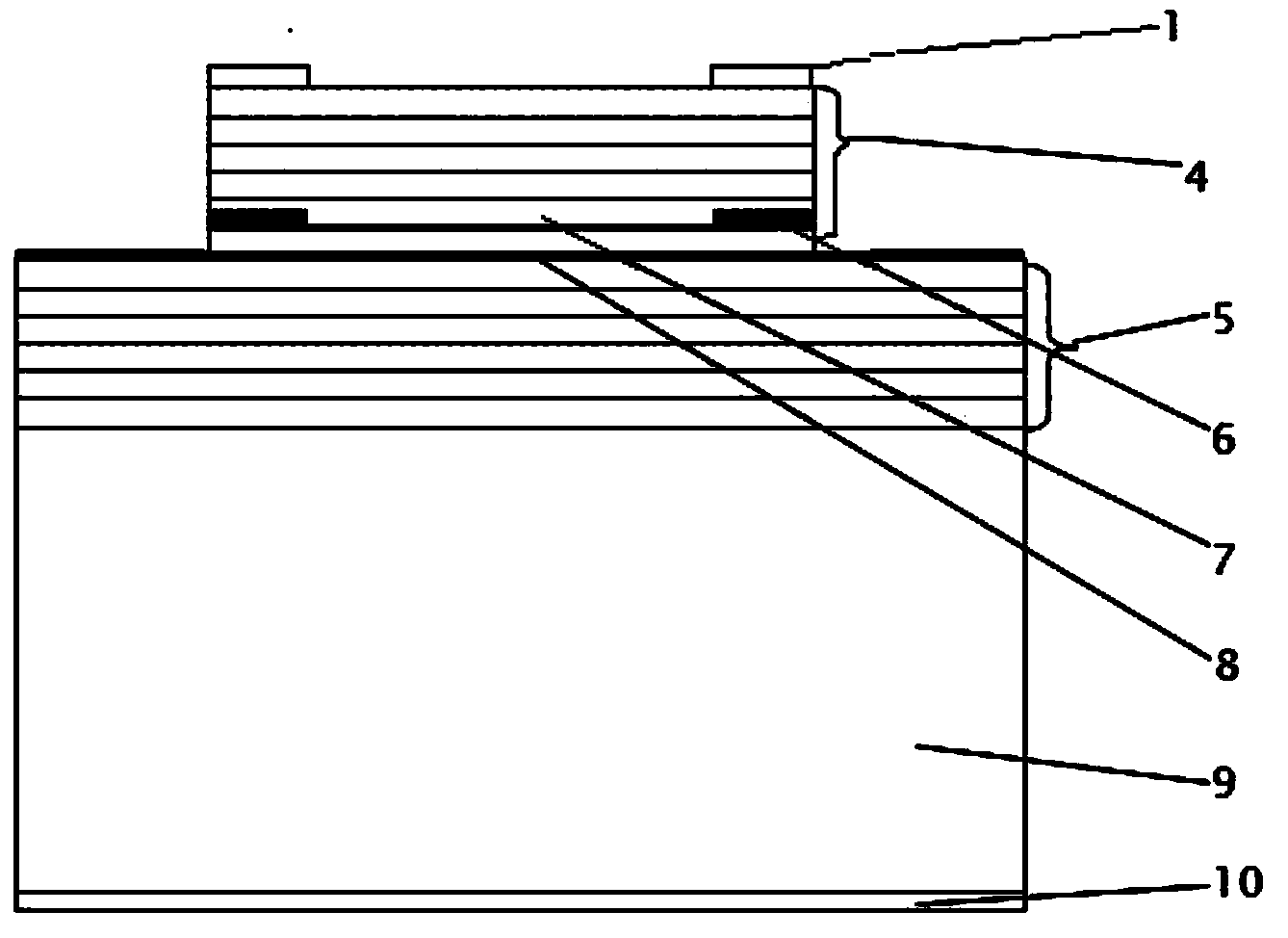
[0032] Step 1. Cleaning the epitaxial wafer, performing photolithography and development on the p-side of the cleaned epitaxial wafer for the first time, and dry-etching the p-side to appear the P-type DBR mesa 4, and the etching depth just reaches the top of the active region 8;

[0033] Wherein, the epitaxial wafer can be obtained by means known to those skilled in the art, and generally adopts commercial purchase;

[0034] Step 2: Perform oxidation measurement on the P-type DBR mesa 4 to obtain an oxidation-limited layer 6 with oxidation holes 7;

[0035] Step 3, thinning and polishing the substrate 9, and then growing an N-face electrode 10 on the surface of the substrate 9;

[0036]Step 4: On the upper surface of the P-type DBR4, grow a transparent insulating dielectric material with an optical thickness that is an odd multiple of a q...

Embodiment 1

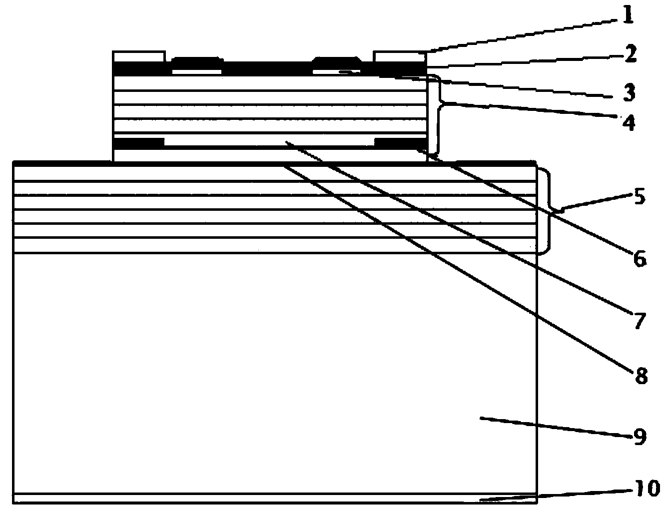
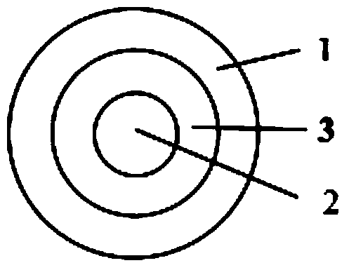
[0040] Such as figure 2 As shown, the vertical cavity surface emitting semiconductor laser includes a P-type DBR4, an active region 8, an N-type DBR5, a substrate 9 and an N-surface electrode 10 arranged in sequence from top to bottom, and a circular oxidation hole is arranged in the P-type DBR4 The oxidation limiting layer 6 of 7 also includes a P-face electrode 1, a transparent conductive film 2 and an annular insulating dielectric film 3, the lower surface of the annular insulating dielectric film 2 is fixed on the upper surface of the P-type DBR4, and blocks the edge of the light exit hole, transparent The conductive thin film 3 is fixed on the upper surface of the annular insulating dielectric film 3 and the exposed P-type DBR4, and blocks the light exit hole, and the P-surface electrode 1 is fixed on the edge of the upper surface of the transparent conductive thin film 3 . The P surface electrode 1 and the annular insulating dielectric film 2 are all in a ring structure...


PUM


Abstract

The invention discloses a vertical-cavity surface-emitting semiconductor laser, and belongs to the technical field of lasers. The laser solves the technical problems that a VCSEL in the prior art is low in single mode output power and poor in single mode stability. The laser comprises a P type DBR, an active region, an N type DBR, a substrate and an N surface electrode, wherein the P type DBR, the active region, the N type DBR, the substrate and the N surface electrode are sequentially and closely arranged from top to bottom, and an oxidation confinement layer with an oxidation hole is arranged in the P type DBR. The laser further comprises a P surface electrode, a transparent conducting thin film and an annular insulating medium film, wherein the annular insulating medium film is fixed to the upper surface of the P type DBR and shields the edge of a light exiting hole, the transparent conducting thin film is fixed to the upper surface of the P type DBR, covers the annular insulating medium film and shields the light exiting hole, and the P surface electrode is fixed to the edge of the upper surface of the transparent conducting thin film and does not shield the light exiting hole. The laser can increase the ground mode output power and improve the reliability.

Description

technical field [0001] The invention relates to a vertical cavity surface emitting semiconductor laser (VCSEL), belonging to the technical field of lasers. Background technique [0002] Due to its good laser stability, coherence and beam quality, single-mode lasers are widely used in communications, printing, pump sources, gas detection and analysis, computer optical mice and other fields. With the further development of these fields, it is required that VCSEL can realize high-power single-mode output. It is widely used in communication, printing, pump source, gas detection and analysis, computer optical mouse and other fields. [0003] In the prior art, there are usually two types of VCSELs to achieve single-mode output: the first way is to increase the mode gain difference so that the gain of the fundamental mode is higher than the gain of the high-order mode, and then through a higher single-mode rejection ratio, the single-mode output is realized. Fundamental mode sing...

Claims


Application Information

Patent Timeline
IPC IPC(8): H01S5/183H01S5/028
Inventor 宁永强李秀山王立军贾鹏刘云秦莉张星
Owner 吉光半导体科技有限公司
Why Eureka
Try Eureka