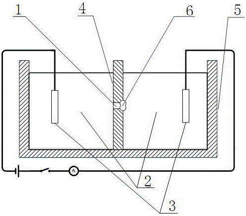
A protein molecular electronic device based on nanopore structure
A nanopore structure, electronic device technology, applied in specific-purpose bioreactors/fermenters, biochemical instruments, biomass post-processing, etc., can solve problems such as poor base sensitivity on nucleic acid chains
- Summary
- Abstract
- Description
- Claims
- Application Information
AI Technical Summary
Problems solved by technology
Method used
Image
Examples
Embodiment approach 1
[0044] Embodiment 1: DNA polymerase molecular electronic device based on nanopore structure
[0045] (1) Preparation of nanopore chips: A series of micro-nano processing methods such as photolithography, dry etching, wet etching, and reactive ion beam etching are used to prepare Si / SiO 2 / SiN suspended support membrane structure. Among them, SiO 2 As an insulating buffer layer, it plays the role of supporting the SiN film and reducing the capacitive effect in electrical measurement. Si mainly supports SiO 2 effect. Finally, a 300kV high-energy focused electron beam (TEM) is used to process a nanohole with a diameter of less than 10 nanometers in the center of the suspended membrane. Processing indicators: nanopore diameter: less than 10 nanometers; thickness: around 50 nanometers.
[0046] (2) The self-made nanopore surface was modified with amino groups. The specific processing procedure is as follows: plasma treatment of self-made nanopore chip for 3 minutes, immersi...
Embodiment approach 2
[0053] Embodiment 2: RNA polymerase molecular electronic device based on nanopore structure
[0054] (1) Preparation of nanopore chips: A series of micro-nano processing methods such as photolithography, dry etching, wet etching, and reactive ion beam etching are used to prepare Si / SiO 2 / SiN suspended support membrane structure. Among them, SiO 2 As an insulating buffer layer, it plays the role of supporting the SiN film and reducing the capacitive effect in electrical measurement. Si mainly supports SiO 2 effect. Finally, a 300kV high-energy focused electron beam (TEM) is used to process a nanohole with a diameter of less than 10 nanometers in the center of the suspended membrane. Processing indicators: nanopore diameter: less than 10 nanometers; thickness: around 50 nanometers.
[0055] (2) The self-made nanopore surface was modified with amino groups. The specific processing procedure is as follows: the self-made nanopore chip is subjected to plasma treatment for 3...
Embodiment approach 3
[0062] Embodiment 3: Urease molecular electronic device based on nanopore structure
[0063] (1) Preparation of nanopore chips: A series of micro-nano processing methods such as photolithography, dry etching, wet etching, and reactive ion beam etching are used to prepare Si / SiO 2 / SiN suspended support membrane structure. Among them, SiO 2 As an insulating buffer layer, it plays the role of supporting the SiN film and reducing the capacitive effect in electrical measurement. Si mainly supports SiO 2 effect. Finally, a 300kV high-energy focused electron beam (TEM) is used to process a nanohole with a diameter of less than 10 nanometers in the center of the suspended membrane. Processing indicators: nanopore diameter: less than 10 nanometers; thickness: around 50 nanometers.
[0064] (2) The self-made nanopore surface was modified with amino groups. The specific processing procedure is as follows: plasma treatment of self-made nanopore chip for 3 minutes, immersion in aq...
PUM
| Property | Measurement | Unit |
|---|---|---|
| size | aaaaa | aaaaa |
| thickness | aaaaa | aaaaa |
Abstract
Description
Claims
Application Information
