Mask graphic defect detection method and mask graphic defect detection system for

A mask pattern and mask image technology, applied in the field of mask pattern defect detection, can solve the problems of complex structure, high cost, high cost of mask pattern defect detection, etc., and achieve the effect of remarkable effect and lower production cost.

Inactive Publication Date: 2015-01-28
SEMICON MFG INT (SHANGHAI) CORP +1
View PDF6 Cites 20 Cited by
  • Summary
  • Abstract
  • Description
  • Claims
  • Application Information

AI Technical Summary

Problems solved by technology

However, the traditional detection method of mask pattern defects using AIMS is technically complicated. After the era of sub-65nm technology nodes, the AIMS system needs to introduce the immersion method to detect the mask pattern defects of 45nm and higher-order nanoscale nodes
The structure of this AIMS system with immersion is very complicated, and it is very expensive to purchase a simulation wafer printer equipped with an AIMS system with immersion function, which makes the detection cost of mask pattern defects too high

Method used


Image

  • Mask graphic defect detection method and mask graphic defect detection system for
  • Mask graphic defect detection method and mask graphic defect detection system for
  • Mask graphic defect detection method and mask graphic defect detection system for

Examples


Embodiment Construction

[0035] In the following description, numerous specific details are given in order to provide a more thorough understanding of the present invention. It will be apparent, however, to one skilled in the art that the present invention may be practiced without one or more of these details. In other examples, in order to avoid confusion with the present invention, some technical features known in the art are described.

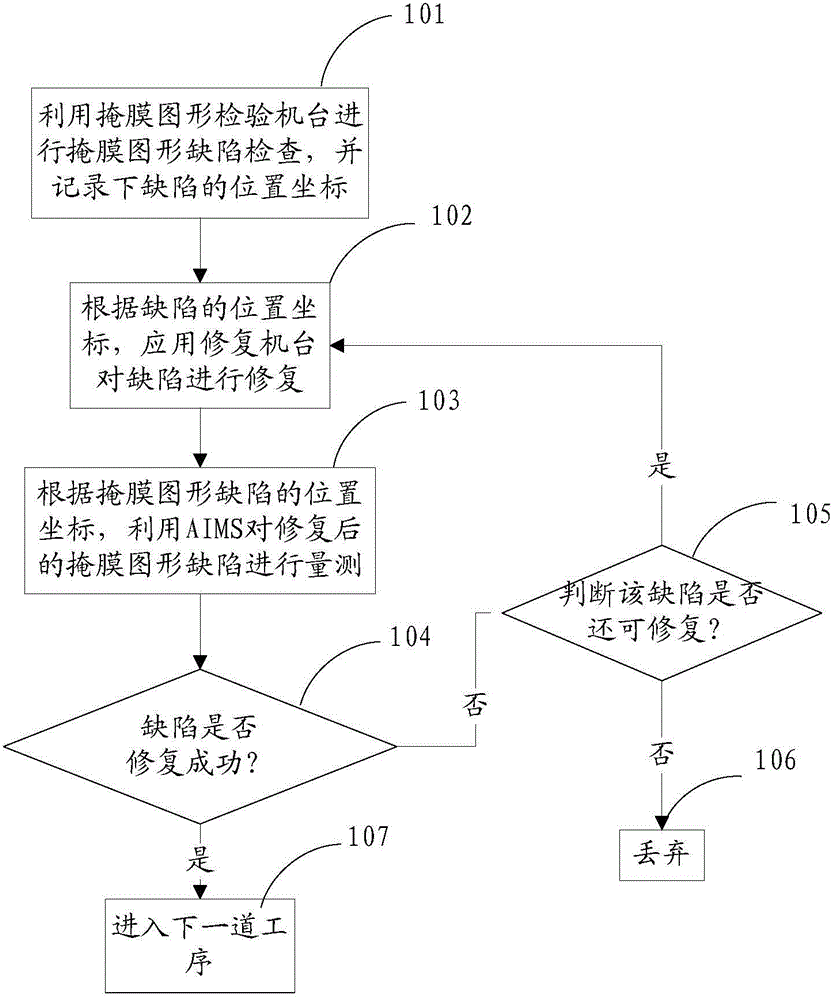
[0036] In the prior art, after the photolithography mask is fabricated, the photolithography mask first needs to be put into a mask pattern inspection machine for pattern defect inspection. The inspection machine checks out the mask pattern defect on the photolithography mask plate, and records the position coordinates of the mask pattern defect. For example, the KLA586 inspection machine provided by KLA-Tencor, California, USA is used to inspect the mask pattern defects on the photolithography mask plate, and at the same time, the KLA586 inspection machine record...


PUM


Abstract

The invention relates to a mask graphic defect detection method and a mask graphic defect detection system. The method comprises the steps of acquiring a mask image, namely obtaining a mask image to be detected and a normal mask image; extracting characteristics and converting formats, namely extracting edge characteristics and converting the edge characteristics into a geometric figure format for storage; performing filling, namely filling a blank region in a rectangular edge contour in a geometric figure; combining data, namely stacking the figures; simulating the contour, namely simulating the contour of a wafer; analyzing the key size of the simulated contour, namely measuring the key size, and calculating a difference value of the key size; and performing judgment, namely judging whether the mask defect is successfully restored according to the difference value of the key size. The invention further relates to the mask graphic defect detection system. The method and the system are simple and easy to implement and are obvious in effect; furthermore, the manufacturing cost of a photoetching mask plate manufacturing technology in the 45nm and even higher-order nano-level photoetching technology is effectively lowered.

Description

technical field [0001] The invention relates to the technical field of semiconductor integrated circuit manufacturing, in particular to a method and system for detecting mask pattern defects in a photolithography mask preparation process. Background technique [0002] Semiconductor integrated circuits (Integrated Circuit, referred to as IC), that is, semiconductor chips, need to go through multiple processes such as material preparation, plate making, photolithography, cleaning, etching, doping, and chemical mechanical polishing during the manufacturing process. most critical. The lithography process determines the advanced level of the semiconductor chip manufacturing process. It is precisely because of the great progress of the lithography technology that the integrated circuit manufacturing process has been brought from the micron era to the deep submicron era, and then into the nanometer era. The photolithography process requires a complete set (several pieces or up to ...

Claims


Application Information

Patent Timeline
Patent Type & Authority Applications(China)
IPC IPC(8): G03F1/44G03F1/72G01N21/956
CPCG03F1/44G01N21/956G03F1/72
Inventor 郭贵琦赵蓓
Owner SEMICON MFG INT (SHANGHAI) CORP
Why Eureka
Try Eureka