Epitaxial growth method for improving LED lighting efficiency

A technology of epitaxial growth and luminous efficiency, applied in the direction of electrical components, circuits, semiconductor devices, etc., can solve the problems of low hole migration ability, reduced luminous efficiency, and inability to migrate, and achieve the effect of improving luminous efficiency

Inactive Publication Date: 2015-02-04
西安利科光电科技有限公司
View PDF3 Cites 13 Cited by
  • Summary
  • Abstract
  • Description
  • Claims
  • Application Information

AI Technical Summary

Problems solved by technology

Among them, the multi-quantum well layer is the core of light emission. Generally speaking, the main light-emitting layer of the multi-quantum well layer is a pair or two pairs of quantum wells close to P-GaN, and the remaining quantum wells do not contribute much to the light

Method used


Image

  • Epitaxial growth method for improving LED lighting efficiency
  • Epitaxial growth method for improving LED lighting efficiency

Examples


Embodiment 1

[0024] Embodiment one (the present invention)

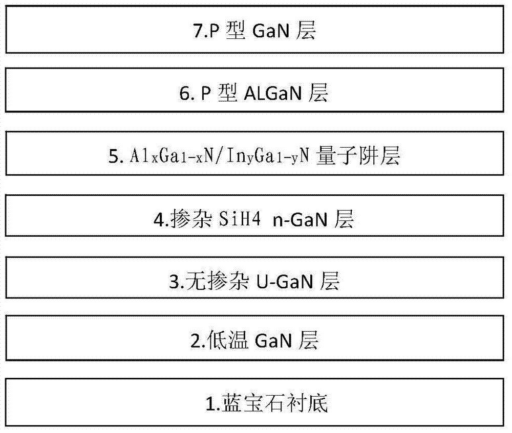
[0025] 1. Put the cleaned sapphire substrate into the MOCVD equipment and bake it at 1100°C for 10 minutes.

[0026] 2. A low-temperature GaN layer with a thickness of 10 nm is grown at a cooling temperature of 620° C., and the growth pressure is 500 torr.

[0027] 3. Raise the temperature to 1165°C to grow an undoped u-GaN layer with a thickness of 1.5um, and the growth pressure is 200torr.

[0028] 4. Raise the temperature to 1170°C, grow a silane-doped n-GaN layer with a thickness of 2.0um, and grow at a growth pressure of 200torr.

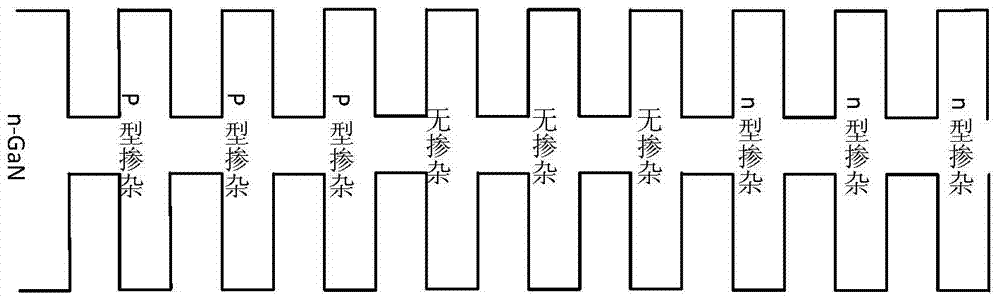
[0029] 5. Switch the carrier gas from hydrogen to nitrogen at a pressure of 200torr to grow AlxGa1-xN / InyGa1-yN multiple quantum well layers. Lower the temperature to 1075°C to grow an InyGa1-yN quantum well layer with a thickness of 3nm; then raise the temperature to 1165°C to grow an AlxGa1-xN quantum barrier layer with a thickness of 10nm to complete the growth of a pair of quantum wells. Th...

Embodiment 2

[0033] Embodiment 2 (traditional solution)

[0034] 1. Put the cleaned sapphire substrate into the MOCVD equipment and bake it at 1100°C for 10 minutes.

[0035] 2. A low-temperature GaN layer with a thickness of 10 nm is grown at a cooling temperature of 620° C., and the growth pressure is 500 torr.

[0036] 3. Raise the temperature to 1165°C to grow an undoped u-GaN layer with a thickness of 1.5um, and the growth pressure is 200torr.

[0037] 4. Raise the temperature to 1170°C, grow a silane-doped n-GaN layer with a thickness of 2.0um, and grow at a growth pressure of 200torr.

[0038] 5. Switch the carrier gas from hydrogen to nitrogen at a pressure of 200torr to grow AlxGa1-xN / InyGa1-yN multiple quantum well layers. Lower the temperature to 1075°C to grow an InyGa1-yN quantum well layer with a thickness of 3nm; then raise the temperature to 1165°C to grow an AlxGa1-xN quantum barrier layer with a thickness of 10nm to complete the growth of a pair of quantum wells. Then ...


PUM

PropertyMeasurementUnit
Doping concentrationaaaaaaaaaa

Abstract

The invention provides a novel LED epitaxial growth method which can effectively improve the lighting efficiency of LED epitaxial structures. The method comprises the links of N-GaN layer growth, multi-quantum well layer growth and P-GaN layer growth, wherein the multi-quantum well layer is of a structure of a plurality of pairs of AlxGa <1-x> N/InyGa <1-y> N, wherein x is more than 0 and less than 1, and y is more than 0 and less than 1; the multi-quantum well layer growth link includes three growth stages in sequence, wherein the AlxGa1-xN quantum barrier is subjected to p type doping in the first stage, the AlxGa1-xN quantum barrier is not doped in the second stage, and the AlxGa1-xN quantum barrier is subjected to n type doping in the third stage; a p type doped AlGaN stopping layer grows, and then the P-GaN layer growth link is performed.

Description

Technical field: [0001] The invention belongs to the preparation technology of semiconductor electronic devices, and in particular relates to a new LED epitaxial growth method. Background technique: [0002] LED lighting has become the third generation of high-efficiency light sources after incandescent lamps and energy-saving lamps due to its high luminous efficiency, long service life, strong safety and reliability, energy saving and environmental protection. At present, LEDs have been widely used in the fields of traffic lights, automobile tail lights, advertising display screens, mobile phone TV backlights and white lighting. The production of a normal LED lamp bead generally goes through the following steps: epitaxial growth section, chip section and packaging section. Among them, the epitaxial growth section determines the brightness of LEDs exceeding 80%, which is the core technology of the entire industrial chain. Epitaxial growth is to use MOCVD technology to desi...

Claims


Application Information

Patent Timeline
IPC IPC(8): H01L33/30H01L33/26H01L33/00
CPCH01L33/005H01L33/04H01L33/32H01L2933/0008
Inventor 商毅博
Owner 西安利科光电科技有限公司
Why Eureka
Try Eureka