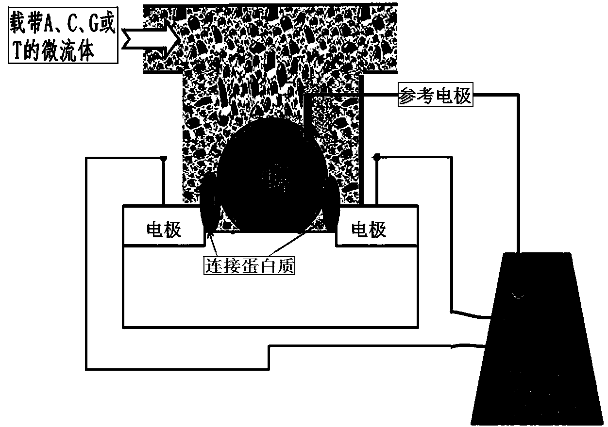
Single-molecule nucleic acid sequencing device based on nanometer counter electrodes
A molecular nucleic acid and electrode technology, applied in the field of single-molecule nucleic acid sequencing devices based on nano-counter electrodes, to achieve the effects of improving sequencing speed, overcoming sequencing bias, and low-cost sequencing
- Summary
- Abstract
- Description
- Claims
- Application Information
AI Technical Summary
Problems solved by technology
Method used
Image
Examples
Embodiment approach 1
[0044] Embodiment 1: Single-molecule nucleic acid sequencing device based on nano-counter electrodes
[0045] (1) Preparation of gold nano-counter electrode: The nano-electrode pair chip is prepared on a silicon chip by conventional photolithography process. The process includes oxidation, glue coating, electron beam exposure, metal deposition, PR cleaning, BOE etching, and again Glue coating and electron beam exposure were used to prepare nano-gold electrode pairs with exposed tips. The processing index is: the electrode width is 50 nanometers, the gap is 10 nanometers; the SiO2 layer is 150 nanometers.
[0046] (2) Insulation modification of the surface of the gold nanoelectrode: the surface of the gold electrode was modified with thioglycolic acid aqueous solution / hexadecane mercaptan ethanol solution, and an insulating layer was constructed on the electrode surface. Soak in solution for 5 minutes; soak in deionized water for 5 minutes; soak in absolute ethanol for short-t...
Embodiment approach 2
[0052] Embodiment 2: Single-molecule nucleic acid sequencing device based on nano-counter electrodes
[0053] (1) Preparation of platinum nano-counter electrode: The nano-electrode pair chip is prepared on a silicon chip using a conventional photolithography process. The process includes oxidation, glue coating, electron beam exposure, metal deposition, PR cleaning, BOE etching, and again Glue coating and electron beam exposure are used to prepare exposed nano-gold electrode pairs, and a platinum layer of several nanometers is further deposited on the nano-gold electrode pairs. The processing index is: the electrode width is 50 nanometers, the gap is 10 nanometers; the SiO2 layer is 150 nanometers.
[0054] (2) Insulation modification on the surface of platinum nanoelectrodes: The surface of gold electrodes was modified with thioglycolic acid aqueous solution / hexadecanethiol ethanol solution, and an insulating layer was constructed on the electrode surface. The specific proce...
Embodiment approach 3
[0060] Embodiment 3: Single-molecule nucleic acid sequencing device based on nano-counter electrodes
[0061] (1) Preparation of palladium nano-counter electrode: The nano-electrode pair chip is prepared on the silicon chip by conventional photolithography process. The process includes oxidation, glue coating, electron beam exposure, metal deposition, PR cleaning, BOE etching, and again Glue coating and electron beam exposure were used to prepare exposed gold nano-electrode pairs. A palladium layer of several nanometers is further deposited on the nano-gold electrode pair. The processing index is: the electrode width is 50 nanometers, the gap is 10 nanometers; the SiO2 layer is 150 nanometers.
[0062] (2) Insulation modification on the surface of the palladium nanoelectrode: the surface of the gold electrode was modified with thioglycolic acid aqueous solution / hexadecane mercaptan ethanol solution, and an insulating layer was constructed on the electrode surface. The specif...
PUM
 Abstract
Description
Claims
Application Information
 - R&D
- Intellectual Property
- Life Sciences
- Materials
- Tech Scout
- Unparalleled Data Quality
- Higher Quality Content
- 60% Fewer Hallucinations
Browse by: Latest US Patents, China's latest patents, Technical Efficacy Thesaurus, Application Domain, Technology Topic, Popular Technical Reports.
© 2025 PatSnap. All rights reserved.Legal|Privacy policy|Modern Slavery Act Transparency Statement|Sitemap|About US| Contact US: help@patsnap.com

