
Vanadium compensated, SI SiC single crystals of NU and PI type and the crystal growth process thereof

A crystal growth, single crystal technology, applied in the direction of single crystal growth, single crystal growth, crystal growth, etc., can solve the problems of SiC crystal 17 pollution and so on

Active Publication Date: 2015-02-18
II VI
View PDF15 Cites 9 Cited by
  • Summary
  • Abstract
  • Description
  • Claims
  • Application Information

AI Technical Summary

Problems solved by technology

However, these common measures are only partially effective, and contamination of the grown SiC crystal17 with nitrogen remains a problem

Method used


Image

  • Vanadium compensated, SI SiC single crystals of NU and PI type and the crystal growth process thereof
  • Vanadium compensated, SI SiC single crystals of NU and PI type and the crystal growth process thereof
  • Vanadium compensated, SI SiC single crystals of NU and PI type and the crystal growth process thereof

Examples


Embodiment Construction

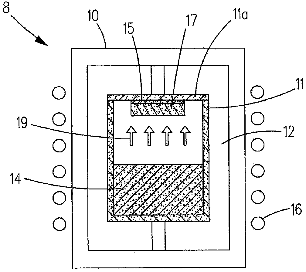
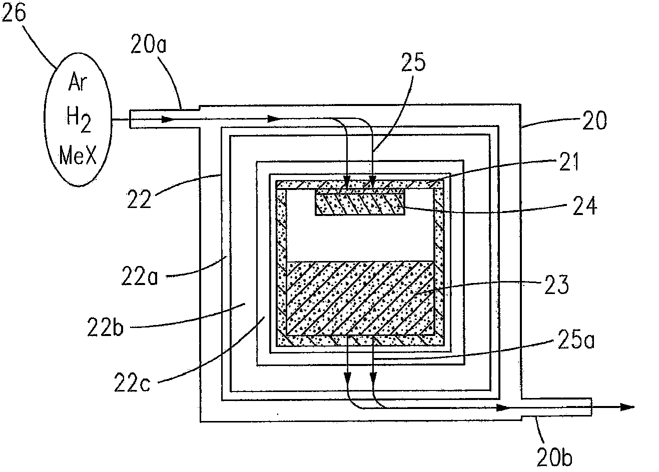
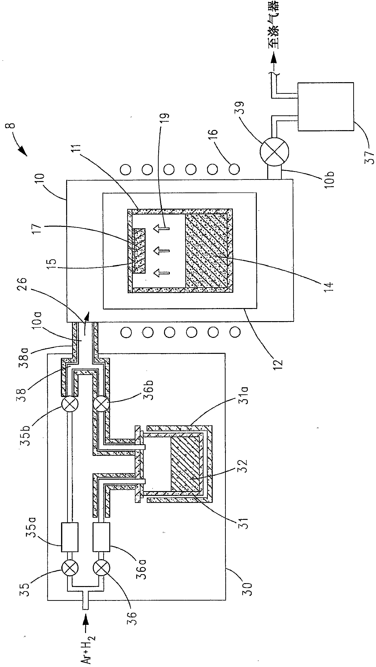
[0104] The SiC growth method described hereinafter incorporates conventional elements of the prior art, such as the use of halogen-purified graphite, vacuum evacuation of the pre-growth, and growth under continuous purge with high-purity inert gases. Furthermore, the SiC growth method described below includes the following new elements:

[0105] 1. Growth under a reactive atmosphere that results in the removal of remaining background nitrogen and boron from the growth environment by chemical bonding.

[0106] 2. A two-stage process for the growth of PI-type SI SiC crystals, comprising removing background nitrogen (N) and background boron (B) from the growth environment in stage (a), followed by, in stage (b), using The grown crystals are grown by controlled co-doping of vanadium (V) and B.

[0107] 3. A two-stage method for the growth of NU-type SI SiC crystals, comprising the removal of N and B from the growth environment in stage (a), followed by, in stage (b), the use of V...


PUM


Abstract

In a crystal growth apparatus and method, polycrystalline source material and a seed crystal are introduced into a growth ambient comprised of a growth crucible disposed inside of a furnace chamber. In the presence of a first sublimation growth pressure, a single crystal is sublimation grown on the seed crystal via precipitation of sublimated source material on the seed crystal in the presence of a flow of a first gas that includes a reactive component that reacts with and removes donor and / or acceptor background impurities from the growth ambient during said sublimation growth. Then, in the presence of a second sublimation growth pressure, the single crystal is sublimation grown on the seed crystal via precipitation of sublimated source material on the seed crystal in the presence of a flow of a second gas that includes dopant vapors, but which does not include the reactive component.

Description

technical field [0001] The present invention relates to silicon carbide single crystals, in particular vanadium compensated semi-insulating (hereinafter 'SI) SiC single crystals of the 4H and 6H polytypes intended for use in semiconductor, electronic and optoelectronic devices. Background technique [0002] Definitions: The following definitions will be used in this article. [0003] donor . Impurities in semiconductors capable of donating electrons to conduction band (hereafter 'CB) or other levels of the band gap are called donors. [0004] recipient . Impurities in semiconductors that are capable of trapping electrons from the valence band (hereafter 'VB) or other energy levels of the band gap are called acceptors. [0005] shallow donor . Donors that ionize heavily at room temperature are called shallow donors. Nitrogen (N) is a group V element of the periodic table having 5 valence electrons. In the SiC lattice, N replaces C and donates four electrons to form...

Claims


Application Information

Patent Timeline
Patent Type & Authority Applications(China)
IPC IPC(8): C30B23/02C30B29/36
CPCC30B29/36H01B3/025C30B23/002
Inventor 伊利亚·茨维巴克托马斯·E·安德森阿维纳什·K·古普塔瓦拉特哈拉詹·伦加拉詹加里·E·鲁兰安德鲁·E·索齐斯P·吴X·徐
Owner II VI
Learn More