Process method of soi LDMOS device preparation

A process method and device technology, applied in the field of semiconductor process manufacturing, can solve the problems of difficult dielectric isolation, low SOI withstand voltage, unfavorable device heat dissipation, etc., and achieve the effects of simple process steps, guaranteed isolation, and simple operation

Active Publication Date: 2017-07-25
58TH RES INST OF CETC
View PDF4 Cites 0 Cited by
  • Summary
  • Abstract
  • Description
  • Claims
  • Application Information

AI Technical Summary

Problems solved by technology

However, limited by the device structure and process, the top silicon layer and the dielectric buried layer cannot be too thick
Because the silicon layer is too thick, it will bring difficulties for dielectric isolation; if the dielectric buried layer is too thick, not only the process implementation is difficult, but also it is not conducive to device heat dissipation, so the longitudinal withstand voltage of SOI is low, which restricts the application of SOI high-voltage integrated circuits

Method used


Image

  • Process method of soi LDMOS device preparation
  • Process method of soi LDMOS device preparation
  • Process method of soi LDMOS device preparation

Examples


Embodiment Construction

[0044] The present invention is described in further detail now in conjunction with accompanying drawing. These drawings are all simplified schematic diagrams, which only illustrate the basic structure of the present invention in a schematic manner, so they only show the configurations related to the present invention.

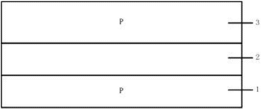
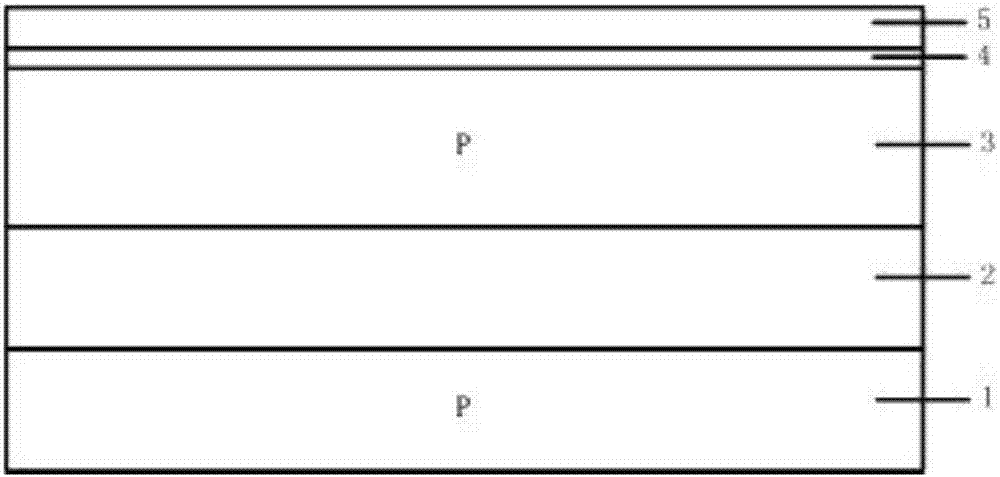
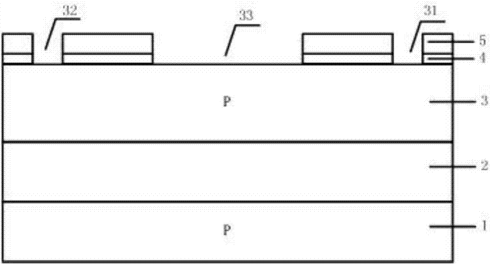
[0045] In an embodiment of a process method for preparing an SOI LDMOS device according to the present invention, the SOI LDMOS device is prepared on the basis of an SOI process base, and the process base includes a silicon substrate 1, a BOX buried Oxygen layer 2 and top silicon film 3. Wherein the resistivity of the top silicon film 3 is 10-40Ω•cm, and the thickness is greater than 1.5µm. Described processing method comprises the steps:

[0046] 1) if figure 1 As shown, a P-type well is implanted in the top silicon film, and the P-well implantation dose is 1e12-1e14cm -2 , to increase the P-type well content in the top silicon film. Step 1) is to prepa...


PUM

PropertyMeasurementUnit
electrical resistivityaaaaaaaaaa
thicknessaaaaaaaaaa
thicknessaaaaaaaaaa

Abstract

The invention relates to a technical method for preparing an SOI LDMOS device. The method comprises the following steps: (1), performing P-type trap injection in a top-layer silicon film; (2), applying an oxidation backflow technology on the top-layer silicon film; (3), using a photoetching technology; (4), employing the photoetching technology and a corrosion technology; (5), utilizing the oxidation backflow technology;(6), employing the corrosion technology; (7), performing N-type trap injection to form an N-type doped area; (8), performing the P-type trap injection to form a first P-type doped area; (9), performing the P-type trap injection to form a second P-type doped area; (10), performing P-type source-drain injection to form a P-type source area and a P-type drain area; (11), performing deposition to form an insulation medium layer; (12), carrying out photoetching corrosion; (13), performing deposition to form a metal layer; (14), and carrying out the photoetching corrosion. The technical method is compatible with a CMOS technical process, the technology is concise and controllable, voltage withstanding performance of the high-voltage SOI LDMOS device can be ensured, and at the same time, isolation between devices can also be ensured.

Description

technical field [0001] The invention relates to a SOI CMOS preparation process method, in particular to a SOI LDMOS device preparation process method, and belongs to the technical field of semiconductor process manufacturing. Background technique [0002] The development of integrated circuits has benefited from the continuous reduction of feature size and the continuous improvement of chip integration. However, the continuous reduction of feature size has brought many new problems in manufacturing materials, device mechanisms and manufacturing processes, which have affected the function of small-size integrated circuits. consumption, reliability, and circuit performance. Researchers have developed various methods to solve these problems, such as deep trench isolation, HALO mechanism, high-K gate dielectric materials, etc., but these technologies cannot be fully applied when the feature size is further reduced. Silicon-on-insulator (SOI) uses the insulating layer to elimina...

Claims


Application Information

Patent Timeline
Patent Type & Authority Patents(China)
IPC IPC(8): H01L21/336H01L29/78
CPCH01L29/66681H01L29/7824
Inventor 郑良晨郑若成洪根深周淼
Owner 58TH RES INST OF CETC
Why Eureka
Try Eureka