Low-temperature polycrystalline silicon thin-film transistor based on dual-gate structure and preparation method thereof

A technology of thin-film transistors and low-temperature polysilicon, applied in the direction of transistors, semiconductor/solid-state device manufacturing, electric solid-state devices, etc., can solve problems such as channel light leakage, and achieve the effects of enhanced charging capacity, small size, and increased pixel aperture ratio

Inactive Publication Date: 2015-03-11
SHENZHEN CHINA STAR OPTOELECTRONICS TECH CO LTD
View PDF5 Cites 29 Cited by
  • Summary
  • Abstract
  • Description
  • Claims
  • Application Information

AI Technical Summary

Problems solved by technology

[0004] An object of the present invention is to provide a low-temperature polysilicon thin film transistor based on a double-gate structure and its method, so as to solve the problem of light leakage in the channel due to the lack of a shileding layer in the LCD display in the prior art

Method used


Image

  • Low-temperature polycrystalline silicon thin-film transistor based on dual-gate structure and preparation method thereof
  • Low-temperature polycrystalline silicon thin-film transistor based on dual-gate structure and preparation method thereof
  • Low-temperature polycrystalline silicon thin-film transistor based on dual-gate structure and preparation method thereof

Examples


Embodiment Construction

[0025] The description of the following embodiments refers to the attached drawings to illustrate specific embodiments that the present invention can be implemented.

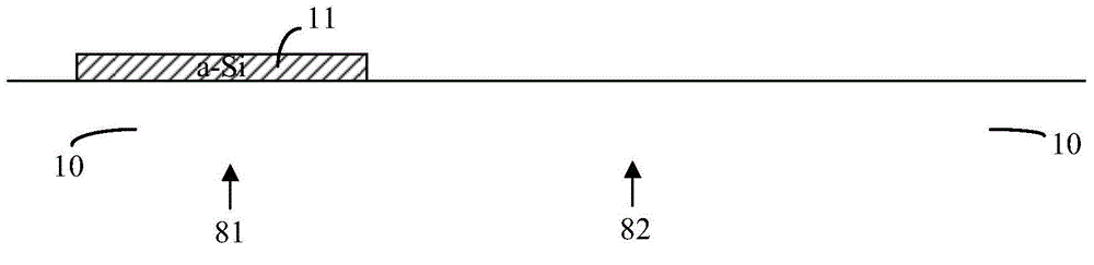
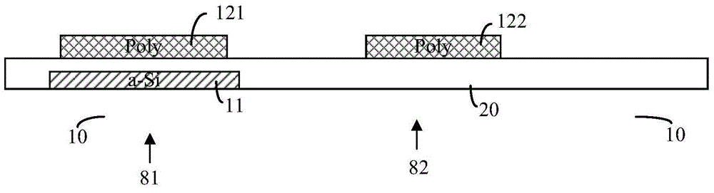
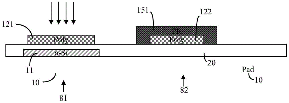
[0026] For an embodiment of the present invention, please refer to Picture 9 , Is a low-temperature polysilicon thin film transistor based on a double-gate structure, including: a substrate 10, at least one patterned amorphous silicon layer 11 (Amorphous silicon, a-si), an N-type metal oxide semiconductor 81 (NMOS), And a P-type metal oxide semiconductor 82 (PMOS). The at least one patterned amorphous silicon layer 11 (Amorphous silicon, a-si) is located in a barrier layer 20 (barrier layer) on the substrate 10, and the at least one patterned amorphous silicon layer 11 forms a Bottom gate; the N-type metal oxide semiconductor 81 is located on the barrier layer 20; and the P-type metal oxide semiconductor 82 is located on the barrier layer 20; wherein, the N The metal oxide semiconductor 81 has a patterned gate e...


PUM


Abstract

The invention discloses a low-temperature polycrystalline silicon thin-film transistor based on a dual-gate structure and a preparation method of the low-temperature polycrystalline silicon thin-film transistor with the dual-gate structure. The low-temperature polycrystalline silicon thin-film transistor comprises a substrate; at least one patterning amorphous silicon layer which is arranged in the barrier layer of the substrate and forms a bottom-gate; an N-channel metal oxide semiconductor which is arranged on the barrier layer; and a P-channel metal oxide semiconductor which is located on the barrier layer, wherein the patterning gate electrode layer formed by the N-channel metal oxide semiconductor and the bottom-gate formed by at least one patterning amorphous silicon layer are combined to form dual-gate structure, so that the current-voltage characteristic is more stable and the breakover current is improved obviously; the driving capacity is increased, the power consumption is reduced and the yield rate of products is improved.

Description

【Technical Field】 [0001] The invention relates to the technical field of liquid crystal production, in particular to a low-temperature polysilicon thin film transistor (LTPS TFT) based on a dual gate structure and a preparation method thereof. 【Background technique】 [0002] Low-temperature polysilicon thin film transistor (LTPS TFT) technology has matured day by day. Its advantage is that compared with amorphous silicon (a-si) and oxide (oxide), it has higher carrier mobility and can enhance display performance Drive ability to reduce power consumption. The low temperature polysilicon thin film transistor (LTPS TFT) process can also be made into a complementary metal oxide semiconductor (Complementary Metal Oxide Semicondutor, CMOS) circuit. The CMOS structure is used in the gate driver on array (GOA) technology to improve the array The reliability of the gate (GOA) circuit. The doping of the lightly doped drain (LDD) of the N-type metal oxide semiconductor (NMOS) in the CMOS ...

Claims


Application Information

Patent Timeline
Patent Type & Authority Applications(China)
IPC IPC(8): H01L29/786H01L21/336
CPCH01L29/6675H01L29/78648H01L29/78672H01L27/1251H01L27/1288H01L29/786H01L21/02118H01L29/7869
Inventor 王笑笑萧祥志杜鹏苏长义徐洪远孙博
Owner SHENZHEN CHINA STAR OPTOELECTRONICS TECH CO LTD
Why Eureka
Try Eureka