
Novel method for improving uniformity and crystallinity of organic-inorganic perovskite thin film

An inorganic calcium and thin film technology, applied in photovoltaic power generation, electrical components, electrical solid devices, etc., can solve the problems of affecting the output voltage, poor film continuity, large surface roughness, etc., to avoid pinhole defects and improve uniformity. , the effect of high uniformity

Inactive Publication Date: 2015-03-11
QINGDAO INST OF BIOENERGY & BIOPROCESS TECH CHINESE ACADEMY OF SCI
View PDF5 Cites 27 Cited by
  • Summary
  • Abstract
  • Description
  • Claims
  • Application Information

AI Technical Summary

Problems solved by technology

The current method 1 has poor continuity of the film and many internal defects in the film; the surface roughness of the method 2 is relatively large, and there are also pinhole-like defect structures, which cause uneven distribution of the built-in electric field in the microscopic area, thus affecting the output. Voltage and other parameters

Method used


Image

  • Novel method for improving uniformity and crystallinity of organic-inorganic perovskite thin film
  • Novel method for improving uniformity and crystallinity of organic-inorganic perovskite thin film
  • Novel method for improving uniformity and crystallinity of organic-inorganic perovskite thin film

Examples


Embodiment 1

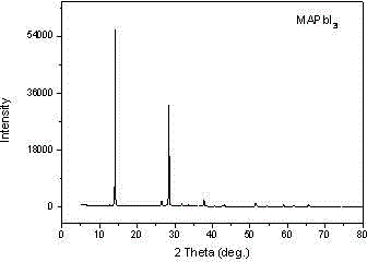
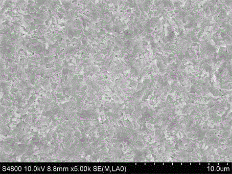
[0020] First, TiO was prepared by sol-gel method 2 Colloid, spin-coated on the cleaned FTO glass, then 500 o C heat treatment for 30 min to obtain dense TiO 2 film. Spin-coating TiO on re-dense thin films 2 Slurry, TiO 2 particle size ~20 nm, and then a further 500 o C heat treatment for 30 min to obtain TiO 2 mesoporous film. Secondly, according to the molar percentage 1:0.5 PbI 2 and PbCl 2 mixed in DMSO solution to prepare a solution with a mass ratio of 40%, and then spin-coated on dense TiO 2 film, heated to 100 o C, 60 min, evaporate the solvent, and finally get MAPbI 3 perovskite structure. Finally, a hole transport layer Spiro-OMeTAD was spin-coated on the perovskite layer, gold electrodes were vapor-deposited, and a solar cell device was assembled to obtain a photoelectric conversion efficiency of 13.2%.

[0021]

Embodiment 2

[0023] First, TiO was prepared by sol-gel method 2 Colloid, spin-coated on the cleaned FTO glass, then 500 o C heat treatment for 30 min to obtain dense TiO 2 film. Secondly, according to the molar percentage 1:0.5 PbI 2 and PbI(OH) were mixed in DMSO solution to prepare a solution with a mass ratio of 40%, and then spin-coated on dense TiO 2 film, heated to 100 o C, 60 min, evaporate the solvent, and finally get MAPbI 3 perovskite structure. Finally, a hole transport layer P3HT was spin-coated on the perovskite layer, and a gold electrode was vapor-deposited to assemble a solar cell device, and a photoelectric conversion efficiency of 12.2% was obtained.


PUM


Abstract

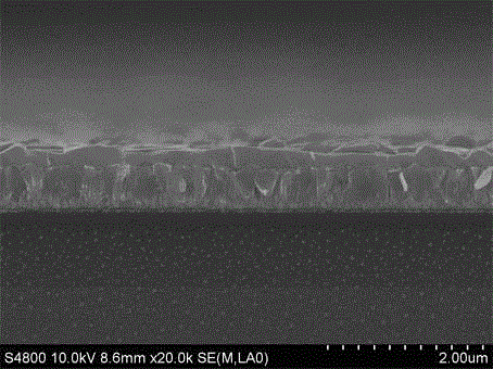
The invention relates to a novel process for preparing an organic-inorganic perovskite thin film through adopting an experimental scheme in which two kinds of metal compounds are adopted as precursors. With the novel process adopted, an efficient solar battery device with a planar structure can be prepared. According to the novel process, the two kinds of metal compound precursors are compounded, and therefore, a pinhole defect of the perovskite thin film can be effectively avoided, and compound of electrons and holes can be alleviated, and short-circuiting risks of the perovskite thin film can be decreased. The novel process of the invention belongs to the photoelectric material field and is characterized in that the two kinds of metal compounds are selected as a source of metal ions in a perovskite material, wherein the general formula of the organic-inorganic perovskite material is ABX3, wherein A is CH3NH3 or NH2-CH=NH2, B is Pb or Sn, and X is I or Br. With the preparation method adopted, the thickness of the perovskite thin film is uniform, and the crystallinity of the perovskite thin film is high, the perovskite thin film can have high electron and hole transport ability. The preparation method is suitable for large-area preparation of organic-inorganic perovskite solar battery devices with planar structures.

Description

technical field [0001] The invention belongs to the technical field of photoelectric materials, and in particular relates to a new method for improving the uniformity and crystallinity of an active layer in a perovskite solar cell. Background technique [0002] Energy is an important material basis for social progress and economic development. With the rapid increase of the world's population and the rapid development of the economies of various countries, the continuous consumption of fossil energy such as coal and oil and the serious pollution problems have seriously affected people's daily life. Life. Speeding up the development of solar cells is one of the effective ways to solve this problem. In the new generation of solar cells, perovskite solar cells have broad application prospects due to their simple preparation process, less raw material consumption, and low cost. Although the current photoelectric conversion efficiency of perovskite cells has reached 15%, it is ...

Claims


Application Information

Patent Timeline
IPC IPC(8): H01L51/48H01L51/42H01L51/46
CPCH10K71/12H10K85/00H10K30/00Y02E10/549
Inventor 崔光磊逄淑平王栋徐红霞张传健
Owner QINGDAO INST OF BIOENERGY & BIOPROCESS TECH CHINESE ACADEMY OF SCI
Learn More