Semiconductor device and method for forming semiconductor device

A semiconductor and device technology, applied in the field of semiconductor manufacturing, can solve the problems of increasing the difficulty of shallow trench isolation structure filling process, and achieve the effects of avoiding breakdown or leakage, improving electrical properties, and small width

Active Publication Date: 2018-12-21
SEMICON MFG INT (SHANGHAI) CORP
View PDF2 Cites 0 Cited by
  • Summary
  • Abstract
  • Description
  • Claims
  • Application Information

AI Technical Summary

Problems solved by technology

However, when the shallow trench width of the shallow trench isolation structure is narrowed, it will cause other negative effects, such as increasing the difficulty of filling the shallow trench isolation structure (gap-filling)

Method used


Image

  • Semiconductor device and method for forming semiconductor device
  • Semiconductor device and method for forming semiconductor device
  • Semiconductor device and method for forming semiconductor device

Examples


no. 1 example

[0049] Figure 6 to Figure 12 It is a schematic cross-sectional structure diagram of the formation process of the semiconductor device according to the first embodiment of the present invention.

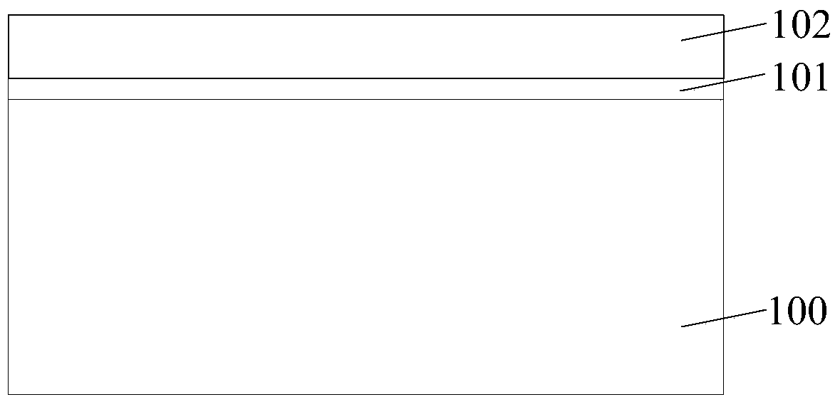
[0050] Please refer to Figure 6 1. A semiconductor substrate 200 is provided. A pad oxide layer 201 and a hard mask layer 202 on the surface of the pad oxide layer 201 are formed on the surface of the semiconductor substrate 200 .

[0051] The semiconductor substrate 200 is used to provide a platform for subsequent processes.

[0052] The semiconductor substrate 200 is one of single crystal silicon, polycrystalline silicon, amorphous silicon or silicon-on-insulator; the semiconductor substrate 200 can also be a Si substrate, a Ge substrate, a GeSi substrate or a GaAs substrate .

[0053] In this embodiment, the semiconductor substrate 200 is a silicon substrate.

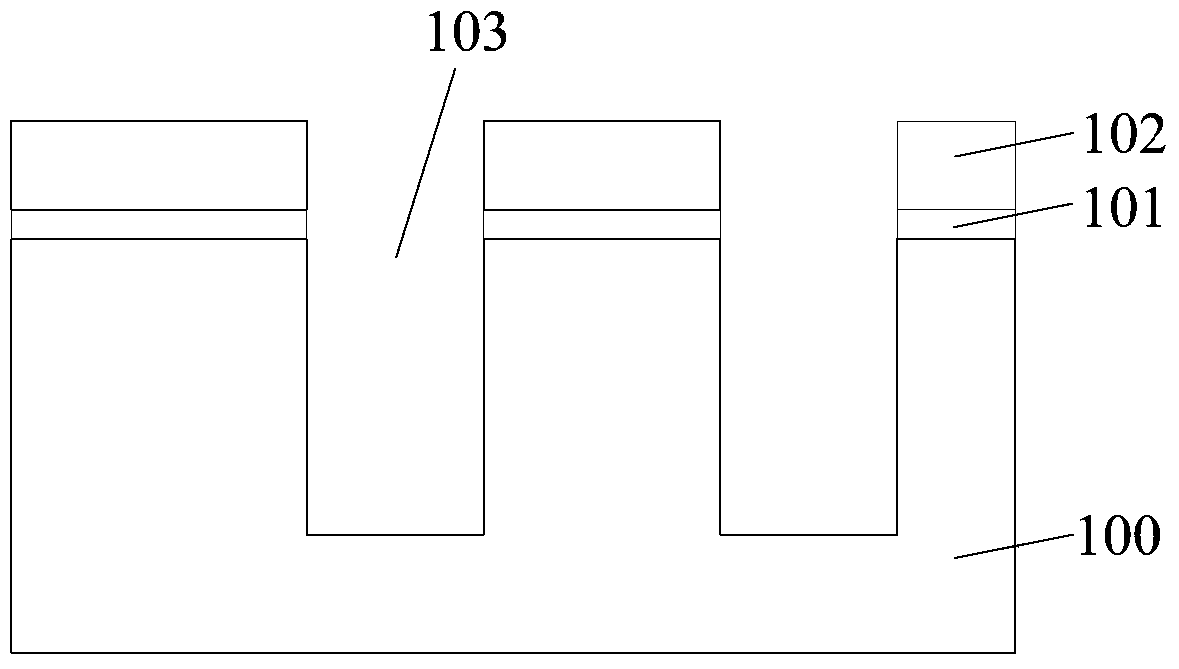
[0054] Active areas (AA: Active Areas) are defined in the semiconductor substrate 200 by a doping process such as an...

no. 2 example

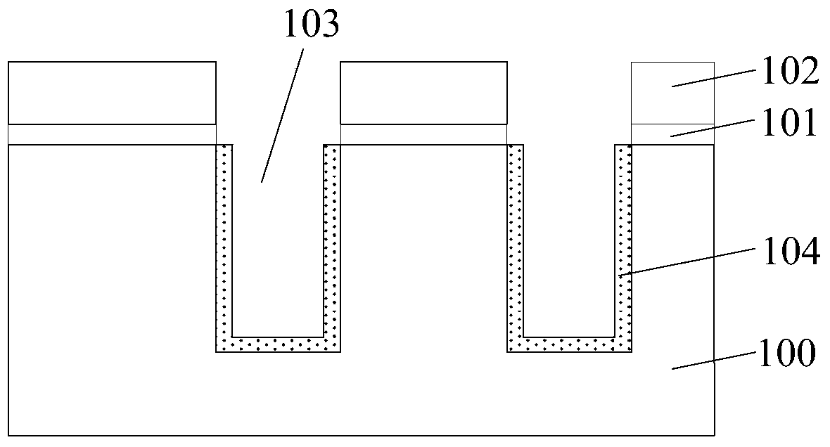
[0118] In the first embodiment, after the epitaxial layer 204 is formed, the hard mask layer 202 and the pad oxide layer 201 are removed. Since the first isolation layer 203 in the shallow trench isolation structure is relatively thin, the first isolation layer 203 will be Etching by the etching process in the subsequent semiconductor device formation process may cause adverse effects.

[0119] In order to avoid the above adverse effects, the present invention also provides a more optimized method for forming a semiconductor device.

[0120] The difference between the second embodiment and the first embodiment is that, before removing the hard mask layer and the pad oxide layer after forming the epitaxial layer, a step is further included: forming a second isolation dielectric layer filling the second trench, The top of the second isolation dielectric layer is flush with the surface of the hard mask layer.

[0121] It should be noted that the formation of the epitaxial layer ...


PUM


Abstract

The invention discloses a semiconductor device and a forming method of the semiconductor device. The forming method of the semiconductor device comprises the following steps: providing a semiconductor substrate, wherein a liner oxide layer and a hard mask layer are formed on the surface of the semiconductor substrate, and the hard mask layer is positioned on the surface of the liner oxide layer; etching the liner oxide layer and the semiconductor substrate of a part of thickness in sequence to form a first channel; laterally etching back a part of hard mask layer on the two sides of the first channel; forming a first isolation layer for filling the first channel; etching back to remove the liner oxide layer and the first isolation layer of a part of thickness until the top of the first isolation layer is lower than the surface of the semiconductor substrate to form a second channel; forming an epitaxial layer on the surface and the side wall of the semiconductor substrate in the second channel, wherein the epitaxial layer and the semiconductor substrate are made of the same material. The formed semiconductor device has larger active region width, and the drive current of the semiconductor device is improved.

Description

technical field [0001] The invention relates to the field of semiconductor manufacturing, in particular to a semiconductor device and a method for forming the semiconductor device. Background technique [0002] The development direction of semiconductor integrated circuits is to increase density and reduce components. Therefore, in the manufacture of integrated circuits, isolation structures are an important technology. The components formed on the semiconductor substrate must be isolated from other components. With the advancement of semiconductor manufacturing technology, the shallow trench isolation (STI: Shallow Trench Isolation) method has replaced the isolation method used in the traditional semiconductor device manufacturing, such as local oxidation method (LOCOS) and other isolation methods. [0003] Compared with other isolation methods, the shallow trench isolation method has many advantages, mainly including: the shallow trench isolation method can obtain a narrow...

Claims


Application Information

Patent Timeline
Patent Type & Authority Patents(China)
IPC IPC(8): H01L21/336H01L29/78H01L21/76
CPCH01L21/76224
Inventor 宋化龙
Owner SEMICON MFG INT (SHANGHAI) CORP
Why Eureka
Try Eureka